Perfecting RF PCB Prototypes with Best DFM Practices

Amit Bahl
CRO
Sierra Circuits
Following design-for-manufacturing (DFM) rules for RF PCBs is critical for avoiding common production errors, such as insufficient annular rings and solder mask clearances.
Addressing these potential manufacturing defects early in the design phase ensures a smooth fabrication process, reducing the risk of board respins and delays.
In this webinar, you will learn the best DFM practices to produce a perfect RF prototype.
Practical DFM tips for designing reliable radio-frequency PCBs
When designing RF boards, you should know your CM’s manufacturing capabilities. Consider their tolerances for trace widths, spacing, and maximum layer counts to ensure the manufacturability of your design.
To facilitate smooth collaboration and a fast turnaround time, submit the required fabrication data, such as Gerber/ODB++/IPC-2581, netlist, BOM, fab, and assembly notes, to your PCB manufacturer in the correct format.
Choose materials that meet the design requirements, considering glass transition temperature (Tg), dissipation factor (Df), dielectric constant (Dk), and mechanical strength. To prevent EMI, implement a symmetrical stack-up with 1 ground plane between 2 signal planes.
For high-current boards, optimize the trace widths based on the copper weight and current-carrying capacity. To avoid etching inaccuracies, maintain at least 7 mil spacing between the copper and board edges.
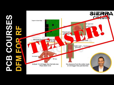
When determining drill-to-copper clearance, consider the drilled hole edge. Maintain at least 8 mil drill-to-copper clearance to avert short circuits.
To address breakout and tangency, provide 2 mil annular rings for laser drilled vias, 3 mil for mechanically drilled vias, and 5 mil for component holes.
Inappropriate clearance between the solder mask edge and surface features leads to solder bridges. Ensure the mask clearances are 2 mil larger than the copper pads. Have 4 mil of mask webs for green and red solder masks and 5 mil for other colors.
Position silkscreen texts beside the pads without overlapping. To ensure legibility, text height and length should be at least 25 mil.
What you’ll learn:
- Common DFM errors that can put your RF job on hold
- Design for manufacturing guidelines for radio frequency PCBs:
- List of production files in the correct format
- Choosing compatible PCB materials
- Designing traces and vias for controlled impedance
- Grounding and shielding: Dos’ and dont’s
- Tips for surface finish, solder mask, and silkscreen
- Manufacturers will love you if you do this
About Amit Bahl
Amit Bahl, widely recognized as the PCB Guy, currently serves as the Chief Revenue Officer at Sierra Circuits. He earned his Bachelor of Science in Engineering from UCLA in 1997, launching his career in Silicon Valley’s tech industry. In 2009, he assumed the role of Director of Sales and Marketing at Sierra Circuits, with a dedicated focus on democratizing design for manufacturing best practices and guidelines for PCB designers and engineers.
Assuming the position of Chief Revenue Officer since 2022, Amit’s mission persists: to simplify the PCB design journey for all stakeholders. His unwavering dedication continues to drive Sierra Circuits as a trusted resource for the PCB design community.
Watch the Trailer