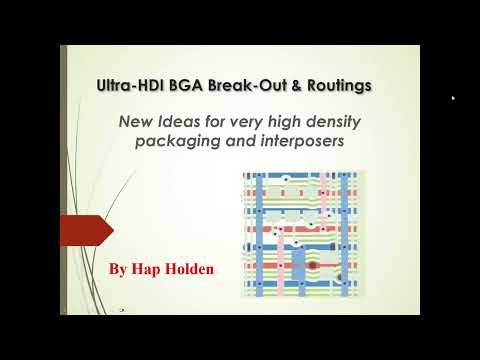
New HDI BGA Breakouts and Routing Strategies

Happy Holden
PCB Technologist and Technical Editor
Iconnect 007
HDI BGA breakouts and routing strategies
This abstract for the webinar on new HDI BGA breakouts and routing strategies was written by Happy Holden:
Although we have been using BGAs for 20 years now, the breakout and routing of them on PCBs has not changed a lot. High-density interconnects and now Ultra-HDI offers alternative strategies that can improve how we route large or fine-pitch BGAs to achieve lower costs, higher performance, or improved reliability. This talk will highlight some of the new techniques and strategies that have been developed for designers that you might not be familiar with.
What you will learn:
- Four strategies developed in Europe and Asia
- Vertical Conductive Structures (VeCS) – A true 3D structure to replace HDI (at lower costs) or with HDI to achieve higher performance
- Integrated Mesh Power Systems (IMPS) – A novel routing structure for high-speed circuitry of only two-metal layers
- Power Mesh for PCBs – An application of IMPS that requires four-layers but is faster and suitable for very high-speed applications
- Channel routing – Taking advantage of chip pin assignments or pin allocations in FPGAs
- Swing via breakouts only practical with HDI
- General advice on routing strategies from Sierra
- Appendix of useful tools
Additional references and reading: Free eBooks on HDI
Appendix of useful tools: Engineering Statistics Handbook
Who should watch this webinar:
PCB designers, purchasing, hardware engineers and project/program managers
About Happy Holden
Happy Holden has spent over 50 years in printed circuit engineering, customer support and product development, with eight of those years in Taiwan, Hong Kong and China He was the CTO of the worlds largest PCB fabricator-Hon Hai Precision Industries-also known as FOXCONN. Prior, he was Senior PCB Technologist for Mentor Graphics’ System Design Division and Development Mgr. for Merix. Before retiring from Hewlett-Packard after 28 years, Holden was responsible for the creation and startup of the NanYa PCB facility in 1984, now the world’s largest organic FC IC substrate fabricator. Holden has a B.S. in chemical engineering from Oregon State University and an M.S. in EE/control theory.


