Design Strategies for Minimizing Jitter and Insertion Loss in High-Speed PCBs

Mike Schnecker
Business Development Manager
Rohde & Schwarz

Amit Bahl
CRO
Sierra Circuits
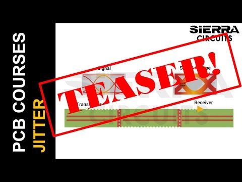
A signal’s deflection from its actual rising and falling edges is called jitter. This might hamper signal synchronization and cause sampling errors. On the other hand, insertion loss refers to signal attenuation as it travels through the transmission lines. Higher insertion loss lowers the signal-to-noise ratio (SNR), making the system prone to noise.
In this webinar, you’ll learn design techniques to tackle jitter and insertion loss. Additionally, we will explain how to detect these signal integrity challenges using eye diagrams and s-parameters.
How to minimize jitter and insertion loss in high-speed PCBs
To design a reliable high-speed PCB, understanding the root causes of signal distortion is crucial. Non-uniform impedance, crosstalk, EMI, and PDN noise are common culprits behind jitter. Whereas, insertion loss arises from conductor, dielectric, radiation, and reflection losses.
The good news is that both jitter and insertion loss can be effectively mitigated using similar design strategies.
Start by choosing the right laminate. Materials with a low dielectric constant (Dk < 4) and low dissipation factor (Df < 0.005) play a pivotal role in minimizing both jitter and insertion loss.
Next, optimize your stack-up. Avoid placing two signal layers adjacently, as this can create unwanted noise and signal coupling. Instead, place signal layers one dielectric away from the reference planes to enhance noise suppression. Ensure a symmetrical build-up and place RF traces on the outer layers to mitigate jitter in high-speed designs.
Maintaining consistent impedance is the key to managing signal losses. Non-uniform impedance causes signal reflections, disrupts timing, and introduces jitter. To avoid these issues, implement series, parallel, Thevenin, or AC trace termination strategies.
To stabilize power supply circuits and address high-frequency clock jitter, deploy decoupling capacitors near IC power pins. Choose capacitors with low ESR and ESL to effectively suppress noise.
Adding guard traces near high-speed signal lines is another effective way to minimize noise coupling. Maintain 3W to 5W spacing between signal and guard traces to reduce crosstalk, and connect guard traces to the ground plane for optimal shielding.
In addition to the above aspects, incorporate solid ground planes without splits. Isolate clock traces from high-current and noisy signals. To ensure low-impedance return paths, implement ground stitching vias around sensitive lines with λ/20 spacing.
When it comes to analysis, you can use eye diagrams, and spectrum analyzers to assess jitter. The width of the eye-opening indicates the amount of clock jitter present in the signal. For insertion loss, evaluate the S21 parameter using a vector network analyzer. The signal loss should remain below 0.1 dB per inch at 5 GHz to ensure efficient signal transmission.
Meet the presenters
Mike Schnecker, Business Development Manager at Rohde & Schwarz
Mike Schnecker has a BS from Lehigh University and an MS from Georgia Tech, both in electrical engineering. His experience in the test and measurement industry includes applications, sales and product development and he has specialized in signal integrity applications using oscilloscopes and other instruments. Prior to joining Rohde & Schwarz, Mr. Schnecker held positions at LeCroy and Tektronix.
Amit Bahl, CRO at Sierra Circuits
Amit Bahl, widely recognized as the PCB Guy, currently serves as the Chief Revenue Officer at Sierra Circuits. He earned his Bachelor of Science in Engineering from UCLA in 1997, launching his career in Silicon Valley’s tech industry. In 2009, he assumed the role of Director of Sales and Marketing at Sierra Circuits, with a dedicated focus on democratizing design for manufacturing best practices and guidelines for PCB designers and engineers.
Assuming the position of Chief Revenue Officer since 2022, Amit’s mission persists: to simplify the PCB design journey for all stakeholders. His unwavering dedication continues to drive Sierra Circuits as a trusted resource for the PCB design community.
Watch the Trailer