Tools for Designers:
Signal and Plane Layer Estimator
Try This New ToolPCB signal and plane layer estimation is not an exact science, but over the past 40 years, several estimation algorithms have been published and become well-known. Sierra Circuits’ Signal and Plane Layer Estimator uses these algorithms to calculate the minimum number of signal and plane layers required to accomplish all the interconnections in a PCB layout.
We have developed this tool to assist you in the design and development stages of a circuit board. The number of signal and plane layers required determines the overall time and the manufacturing cost. Knowing the right number of required signal/plane layers eases the design process.
What determines the number of signal and plane layers required in a PCB?
There is no particular rule that describes the number of signal layers required for a particular circuit board. It depends on the type, length, width, and shape of the board. It also depends on the number of component pins, trace width and spacing, via pad diameter, keep out areas, etc. Our tool uses the values of these quantities and specifies the number of signal and plane layers, rounded to the nearest integer.
Getting started with the Signal and Plane Layer Estimator

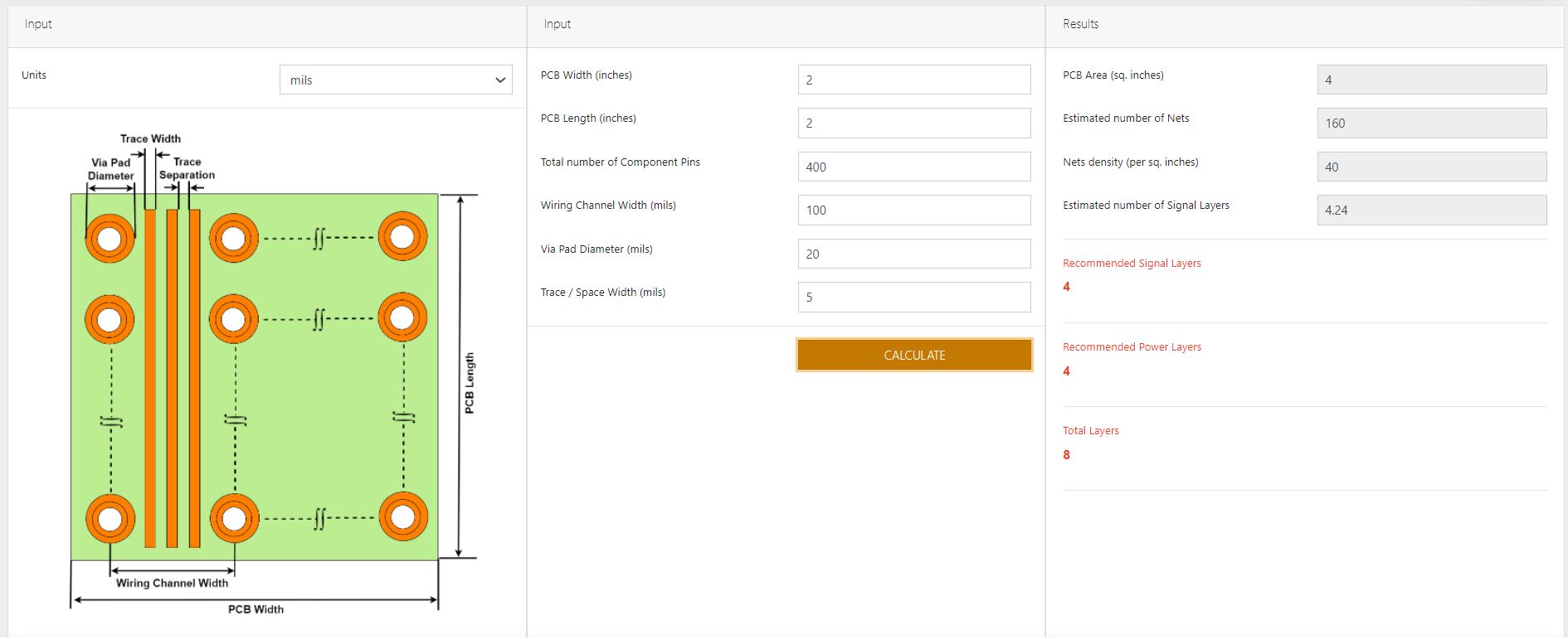
The Signal and Plane Layer Estimator has two sections – input and results. You have to enter all the parameters mentioned in the input section. An illustration of a board with all the input parameters defined is placed on the home page of the calculator.
How to estimate the number of signal/plane layers
Before providing the values, select the unit in which the calculation is to be carried out. By default, the unit is set to mils. Other available options are inches, millimeters, micrometers, and centimeters.
Enter the following required values in the input section:
- PCB width (in inches)
- PCB length (in inches)
- Total number of component pins: Sum total of all pins of the components. Eg: If your board design has got two ICs, one of 8 pins and another of 20 pins, the total number of pins is 28.
- Wiring channel width (in mils): It is assumed here that traces are routed in channels bound by vias on either side. The channel width is the distance between the centers of two vias between which traces will be routed.
- Via pad diameter (in mils)
- Trace/space width (in mils): This is the width of the trace and the space between them.
Next, hit calculate in the results tab. The tool will display the following results in red at the bottom:
- Recommended signal layers
- Recommended plane layers
- Total layers
Along with this, the following values are also obtained:
- PCB area (in sq. inches)
- Estimated number of nets
- Net density (per sq. inches)
We offer an easy-to-use Signal and Plane Layer Estimator that will eliminate your complicated design delays. With the help of this tool, you will be able to understand the required number of signal and plane layers in a go. Keep all the necessary input parameters handy and get a hassle-free estimation in no time.
Watch the tool demo:
Sierra Circuits has developed easy-to-use tools for PCB designers and Electrical Engineers at every stage of circuit board development.
Fabrication, Procurement, & Assembly. PCBs fully assembled in as fast as 5 days.
- Bundled together in an entirely-online process
- Reviewed and tested by Engineers
- DFA & DFM Checks on every order
- Shipped from Silicon Valley in as fast as 5 days
Fabrication. Procurement & Assembly optional. Flexible and transparent for advanced creators.
- Rigid PCBs, built to IPC-6012 Class 2 Specs
- 2 mil (0.002″) trace / space
- DFM Checks on every order
- 24-hour turn-times available
Complex technology, with a dedicated CAM Engineer. Stack-up assistance included.
- Complex PCB requirements
- Mil-Spec & Class 3 with HDI Features
- Blind & Buried Vias
- Flex & Rigid-Flex boards


