Speak to an Account Manager
![]() +1 (800) 763-7503
+1 (800) 763-7503
Tools for Designers:
Sierra Design Portal
The Designer's Best Friend
Cut Down Your Design Time in HalfEmpower your PCB design process
Looking to streamline your PCB development journey? The Sierra Design Portal is your tailored solution, covering all your circuit board requirements, from concept to manufacturing. Featuring a suite of integrated tools and backed by expert services, we guarantee a seamless experience from start to finish.
Why choose Sierra Design Portal?
- Accelerated design process: Streamlines the design process, leading to faster time-to-market for your products.
- Comprehensive toolset: Offers a suite of PCB design tools, technical services, and communication channels all in one place.
- Ready to fab: Guarantees manufacturability, thanks to our expertise in DFM.
Sierra Design Portal Journey
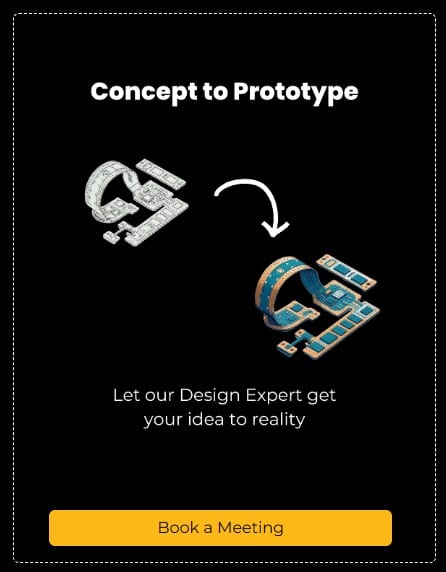
Stage 1: Concept design
Transform your ideas into reality with the guidance of our experienced PCB design engineers. From initial concept to fully realized design, we offer end-to-end services to kick-start your project.
Stage 2: Schematic design
Translate your concepts into well-structured designs with our intuitive tools and expert support.
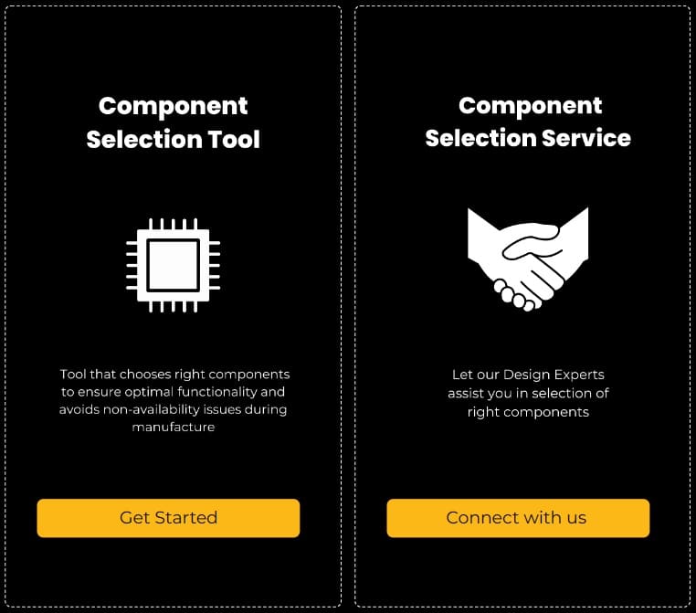
- Component selection: Choose components and their corresponding footprints from our curated library for seamless integration.
- BOM creation: Effortlessly create comprehensive bills of materials with our platform.
- Schematic checklist: Utilize our checklist to enhance design quality and prevent errors.
Stage 3: PCB layout design
Craft a high-quality circuit board layout essential for the functionality and reliability of your devices.
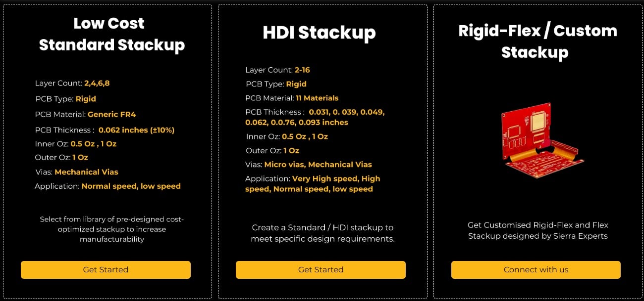
- PCB stack-up design: Build your PCB stack-up with our Stackup Designer, ensuring manufacturability and performance.
- Footprint design: Get an error-free, validated footprint optimized for smooth integration.
- PCB layout design checklist: Identify potential issues using the predetermined checklist.
- BOM validation: Check for duplicate reference designators, bad MPNs, component availability, and other BOM-related issues using our BOM checker.
- Advanced tools: Explore our portfolio of tools, including Material Selector, Impedance Calculator, and more, for comprehensive design analysis.
Stage 4: Ready for manufacturing
Our platform provides comprehensive support, from generating your production files to ensuring the manufacturability of your design.
- Gerber export guide: Seamlessly export your designs with our easy-to-understand guides.
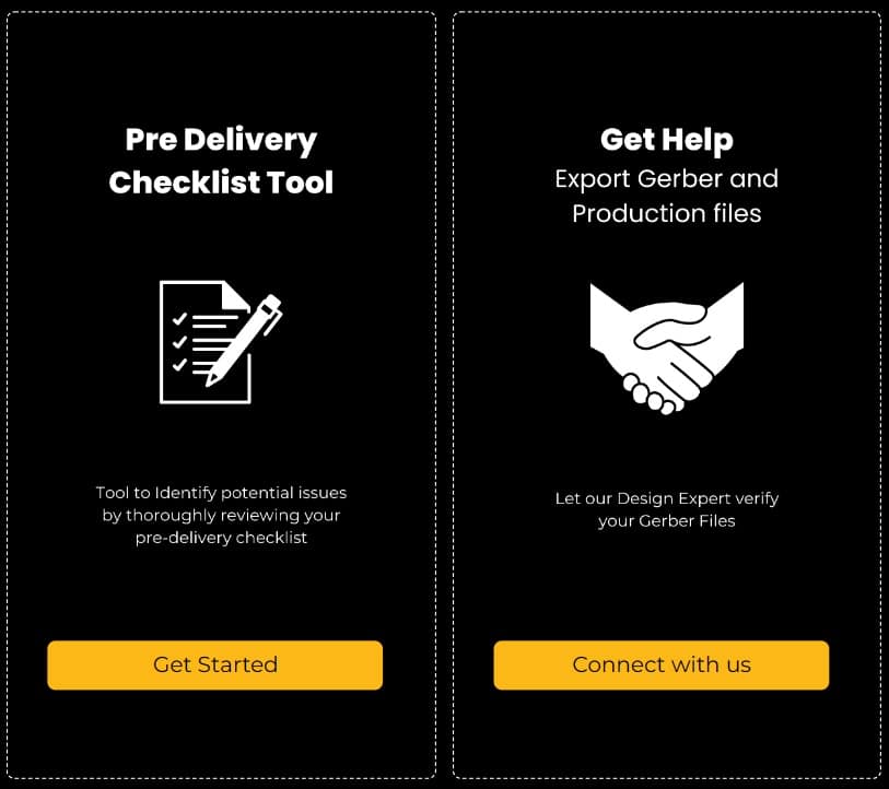
- Pre-delivery checklist: Make sure your designs meet all requirements before submission.
- Gerber check: Validate your designs with precision using our Gerber check tool.
- Sierra’s Better DFM tool: Ensure manufacturability by checking your design with our user-friendly DFM tool.
Ready to turn your concept into reality? Explore our services and start your journey with Sierra Design Portal today.
Sierra Circuits has developed easy-to-use tools for PCB designers and electrical engineers at every stage of circuit board development.


Fabrication, Procurement, & Assembly. PCBs fully assembled in as fast as 5 days.
- Bundled together in an entirely-online process
- Reviewed and tested by Engineers
- DFA & DFM Checks on every order
- Shipped from Silicon Valley in as fast as 5 days

Fabrication. Procurement & Assembly optional. Flexible and transparent for advanced creators.
- Rigid PCBs, built to IPC-6012 Class 2 Specs
- 2 mil (0.002″) trace / space
- DFM Checks on every order
- 24-hour turn-times available

Complex technology, with a dedicated CAM Engineer. Stack-up assistance included.
- Complex PCB requirements
- Mil-Spec & Class 3 with HDI Features
- Blind & Buried Vias
- Flex & Rigid-Flex boards