PCB Stack-Up Design
Before we start the layout design, we will do an in-house PCB stack-up design so that all the design objectives are met. We will also suggest if HDI technology is required or could help in optimization.
Start Your Design QuoteHOW WE CREATE YOUR ERROR-FREE STACK-UP
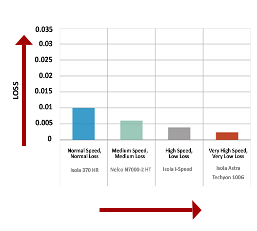
For high-speed and RF boards above 2 GHz, we carefully choose materials with low loss factors.
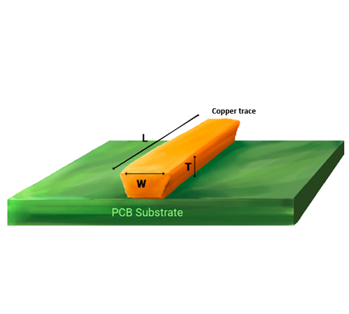
It is a common mistake to think a 4-mil spacing will be sufficient for a 2-oz copper thickness as when we etch the board, thicker the copper, the spacing between the traces will reduce and may become less than the manufacturable limits. Thinner spacing on heavy copper may lead to reworks and delays.
THE
PLUS
Sierra Circuits provides customers with stack-up design recommendations. After you place an order with us, our engineering team reviews your stack-up to ensure it is optimized for PCB manufacturing. If we notice that changes are required for a better fabrication process, we will get back to you with our suggestions.
+

WHY SIERRA
- Successful PCB stack-up design requires close coordination between the layout engineers and the manufacturing team. As we provide layout, stack-up and manufacturing services under one roof, we can deliver error-free stack-ups with the quickest turnarounds possible and you have the guarantee they will be manufacturable.
Other Ways Sierra Circuits Can Help
We have many resources designed to help you, no matter where you are in your journey to becoming a PCB expert.
PCB Manufacturing& Assembly Processes
Knowing how your boards are manufactured and assembled will help you design boards that are cost-effective and technically robust.
Learn PCB ManufacturingSupport
Need help with your Stackup? Want to find out what our chip stock looks like? Have questions about your order? We're here to help.
Contact SupportShare Project with your Engineers
Access Sierra Circuits Project Access (SPX) Portal. Just like our Customer Portal, SPX is encrypted and fully protected.
Visit the SPX PortalTurn-times as fast as 1 day.
Sierra Circuits can manufacture your PCB and have it expedited to you within 24 hours. Full turnkey boards, with assembly and components in as fast as 5 days. Get an Instant, Itemized Quote
Fabrication, Procurement, & Assembly. PCBs fully assembled in as fast as 5 days.
- Bundled together in an entirely-online process
- Reviewed and tested by Engineers
- DFA & DFM Checks on every order
- Shipped from Silicon Valley in as fast as 5 days
Fabrication. Procurement & Assembly optional. Flexible and transparent for advanced creators.
- Rigid PCBs, built to IPC-6012 Class 2 Specs
- 2 mil (0.002″) trace / space
- DFM Checks on every order
- 24-hour turn-times available
Complex technology, with a dedicated CAM Engineer. Stack-up assistance included.
- Complex PCB requirements
- Mil-Spec & Class 3 with HDI Features
- Blind & Buried Vias
- Flex & Rigid-Flex boards


