PCB Layout Design
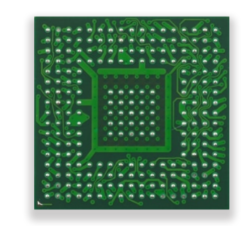
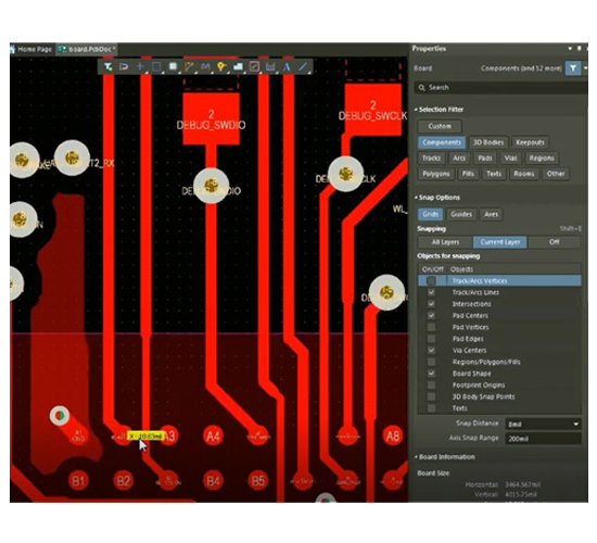
Our PCB layout design services include stack-up design, constraint setting, component placement, routing and Gerber generation handled by a team with 20 years of experience. We specialize in DDR, fine pitch BGA, component placement optimization, constraint settings and much more.
Start Your Layout QuoteLET'S TALK ABOUT OUR EXPERIENCE
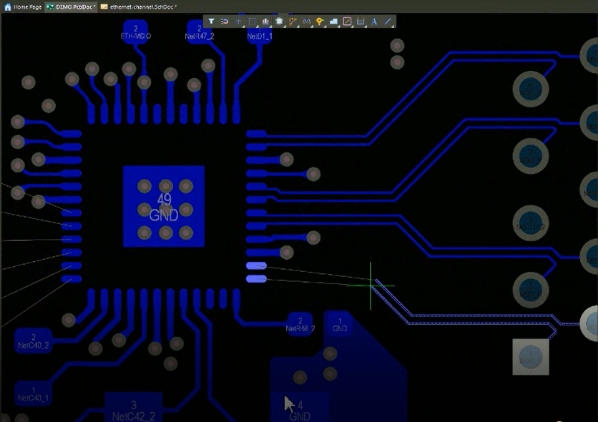
To ensure length matching of signals in the same group, we route them on the same layer.
With our production and layout services under one roof, we can deliver complex designs with faster turnaround times. We drastically reduce the usual back-and-forth between the layout engineers and the fab house.
Component placement optimization reduces the trace lengths and the number of vias, thus the overall cost of the board.
THE
PLUS
We can create your PCB schematic and layout as well as get your board manufactured and assembled under the same roof. This will save you time and ensure an error-free fabrication.
+

WHY SIERRA
- Modern layouts, like high-speed and HDI designs, are very complex and need multiple years of experience. We have listed a few above and there are many more PCB layout design parameters which require high-level skills.
- With design, manufacturing and assembly under one roof, we eliminate miscommunication between different vendors therefore making you save time on your prototype.
Other Ways Sierra Circuits Can Help
We have many resources designed to help you, no matter where you are in your journey to becoming a PCB expert.
PCB Manufacturing& Assembly Processes
Knowing how your boards are manufactured and assembled will help you design boards that are cost-effective and technically robust.
Learn PCB ManufacturingSupport
Need help with your Stackup? Want to find out what our chip stock looks like? Have questions about your order? We're here to help.
Contact SupportShare Project with your Engineers
Access Sierra Circuits Project Access (SPX) Portal. Just like our Customer Portal, SPX is encrypted and fully protected.
Visit the SPX PortalTurn-times as fast as 1 day.
Sierra Circuits can manufacture your PCB and have it expedited to you within 24 hours. Full turnkey boards, with assembly and components in as fast as 5 days. Get an Instant, Itemized Quote
Fabrication, Procurement, & Assembly. PCBs fully assembled in as fast as 5 days.
- Bundled together in an entirely-online process
- Reviewed and tested by Engineers
- DFA & DFM Checks on every order
- Shipped from Silicon Valley in as fast as 5 days
Fabrication. Procurement & Assembly optional. Flexible and transparent for advanced creators.
- Rigid PCBs, built to IPC-6012 Class 2 Specs
- 2 mil (0.002″) trace / space
- DFM Checks on every order
- 24-hour turn-times available
Complex technology, with a dedicated CAM Engineer. Stack-up assistance included.
- Complex PCB requirements
- Mil-Spec & Class 3 with HDI Features
- Blind & Buried Vias
- Flex & Rigid-Flex boards


