Online Printed Circuit Board Fabrication and Assembly


The Pitch
  • Instantly quote and order standard technology
  • Flexible and transparent pricing for fast and easy ordering
  • Prototype with confidence and agility
The Parameters
  • 1 – 1,500 completely assembled boards
  • Built to IPC-6012 Class 2 specs
  • UL Approved
  • Complete DFM check by our CAM engineers
  • Big selection of different surface finishes and materials
  • Edge Plating, Gold Fingers, etc.
Start an Online Quote
LEARN PCB
PCB Manufacturing
PCB Assembly
PCB Design and Layout
PCB Basics
Vias, Drilling & Throughplating
Mechanics
Surface
SMD
Quality
SPECIFICATIONS
PCB Fabrication
STANDARDS & POLICY
PCB Ordering
Policy
Fab + Assembly Capabilities
Summary Our Web PCB service enables ultimate speed and convenience. PCB fabrication: Instantly quote and order standard technology, rigid PCBs up to 12 layers, with standard materials and finishes. These are single lamination PCBs (i.e., no blind/ buried vias allowed). PCB assembly: Instantly quote and order consigned, turnkey and partial-turnkey assembly though the Web PCB service. (Includes instant BOM pricing also!) Note that this service is for rigid PCBs only, not for flex or rigid-flex PCBs.
Data For PCBs: We prefer RS-274X extended Gerber format. If your file is not in RS-274X, send an aperture file. Please see FAQ below for what files to include. For assembly: You will need to upload your BOM (excel format) online for quoting. In the final package, we will need the assembly drawing and XY data.
Turntime 1, 2, 3, 4, 5 and 10 business days from order date. When will my boards ship if I order today?
Cut-off Time 5PM PST.
Minimum Order Quantity/Maximum Order Quantity From 1 PCB to 1500 PCBs. Some restrictions may apply for large quantities on quick turns.
Maximum Board Size Maximum area allowed for a board is 150 square inches. Maximum X or Y dimension allowed is 15.9″ and minimum dimension allowed is 0.5″.
Materials FR4, FR4-06, FR4-lead free. Standard materials are instantly quoted online. Exotic materials may be quoted by a Web Product Specialist offline. Please note that Web PCB service is for rigid PCBs only. For flex or rigid-flex PCBs, please get a custom quote directly through a Sierra sales person
Thickness & Thickness Tolerance Almost all standard thicknesses including 0.062″, 0.031″ etc. (certain layers may be limited to certain standard thicknesses). The tolerance for thickness in Web PCBs is +/- 10% of nominal thickness for boards down to 0.031 thick. For boards less than 0.031 thick, the thickness tolerance is constant at +/- 0.003 (+/- 3 mils).
Arrays Arrays are allowed in Web PCB products. But we will NOT create the arrays for you. Your file has to have the array as a single-up image! When quoting, you will have to enter the array dimensions, how many boards per array, and individual board dimensions. For PCB quotes purpose, always enter the quantity of individual boards (NOT the quantity of arrays). Arrays may have scoring or route and retain.
Minimum Trace & Space Now allowing down to 4 mils (0.004″) minimum trace/space.
Preferred Manufacturing Criteria Minimum air-gap of 0.004″ (space between any two copper features). Minimum annular ring of 0.005″ (applies to both plated and non-plated holes). Minimum inner layer drill-to-copper spacing of 0.013″ (applies to both plated and non-plated holes).
Standard Copper Overplate Surface pattern: Nominal 1 oz/sq foot (0.0013″ to 0.002″) (33 microns to 51 microns)
Copper Plating Inner layer copper: 0.5 oz or 1 oz. Outer layer (finished) copper: 1 oz or 2 oz.
Plating on Hole Walls 0.0008″ to 0.0012″ (20 microns to 30 microns).
Surface Finish HASL (solder), hard gold, bondable gold, immersion gold, immersion silver.
Gold Fingers Gold fingers allowed on HASL finish only.
Standard Gold Thickness Soft Bondable Gold Gold thickness: 30 μin (0.76μ) Nickel thickness: – Palladium thickness: – Immersion Gold Gold thickness: 1.5 – 2.8 μin (0.038μ – 0.0711μ) Nickel thickness: 125 μin – 250 μin Palladium thickness: – Hard Gold Gold thickness: 30 μin (0.8μ) Nickel thickness: – Palladium thickness: –
Minimum Hole Size Down to 6 mils (0.006″) finished hole size allowed.
Maximum Hole Size Plated holes: 246 mils (0.246″). Non-plated holes: 199 mils (0.199″).
Maximum Hole Density Instant quote may not be available if hole density exceeds 100 holes/sq inch (total holes on a board/area of board). Our Web Product Specialist may ask for more details before quoting designs with such high hole-density.
Via-in-Pad Features We allow via-in-pad features on your board. The turntime for such jobs will be minimum 5 days for PCB fabrication. (Any assembly turntime is additional.) All vias in such boards will be filled with non-conductive filling.
Minimum Width of Annular Rings 6 mils (0.006″) (We need this minimum annular ring width on your design to ensure there are no breakouts on the pads in the manufactured board). For more details on annular ring requirements CLICK HERE.
Controlled Dielectric Allowed but only for standard available thicknesses.
Controlled Impedance This means in your design, you are specifying the width of certain traces and spacing to achieve a specific resistance. In your impedance modeling, use the Dk for material 370HR. We expect that in your fab drawing, you will have an impedance table that CLEARLY identifies the target impedance(s), the layer(s) on which they exist and the specific trace widths/spaces to be controlled. See a sample format for impedance table. Do note that in this online service, our controlled impedance offering has certain limitations: Only offered for boards up to 6 layers. Only available with +/- 10% tolerance. You can have controlled impedances on up to 4 different layers on your board. On any layer, you can have up to two different controlled impedances. Our engineers will meet your controlled impedance requirements using our own stack-up. (All we need is your controlled impedance info. We do not need and may not use any specific controlled dielectric information you provide.) If your controlled impedance requirements exceed this spec, please ask for a custom quote.
Counterbores/Countersinks Available.
Internal Cutouts/Slots & Notches Up to 10 plated slots allowed per board. Up to 10 non-plated slots allowed per board. (If any of the above allowances are exceeded in your design, we can still process it for a minimum $100 extra lot charge on your order. We will get your approval before doing so.) Up to 10 cutouts allowed per board. Up to 10 notches allowed per board. Minimum inside radius (for any notch, cutout or slot) = 20 mil (0.02″). Minimum width (of any notch, cutout or slot) = 40 mil (0.04″).
Multiple Parts We expect to see a single image of a single PCB, and the vast majority of the orders we see comply with this. However, if your files do have more than one part on it, we will charge you $100 extra on the order ($100 lot charge).
Soldermask Process Solder mask is available in the following colors: green, blue, red, black, white and clear. It is allowed on both sides. In our Web PCB service, we only offer LPI solder mask. Please follow the guidelines given below. 1. LPI solder mask (green, blue, red and clear color) 2. LPI solder mask (black or white color) Note We only offer LPI solder mask in our Web PCB service. If your design forces us to use laser direct imaging LPI (LDI-LPI) solder mask, we will contact you and get approval for a $500 extra charge on your order. In such case, please see design guidelines for LDI-LPI solder mask. 3. LDI-LPI solder mask (green, red and blue color) 4. LDI-LPI solder mask (black color)
Silkscreen/Legend Legend colors available: white, black, yellow. Both sides allowed. (Legend should have minimum 5 mils (0.005″) trace width).
Logo & UL Markings Vendor markings include Company Logo, UL marking, Flammability, etc. Such vendor markings will be put in bottom Silkscreen.
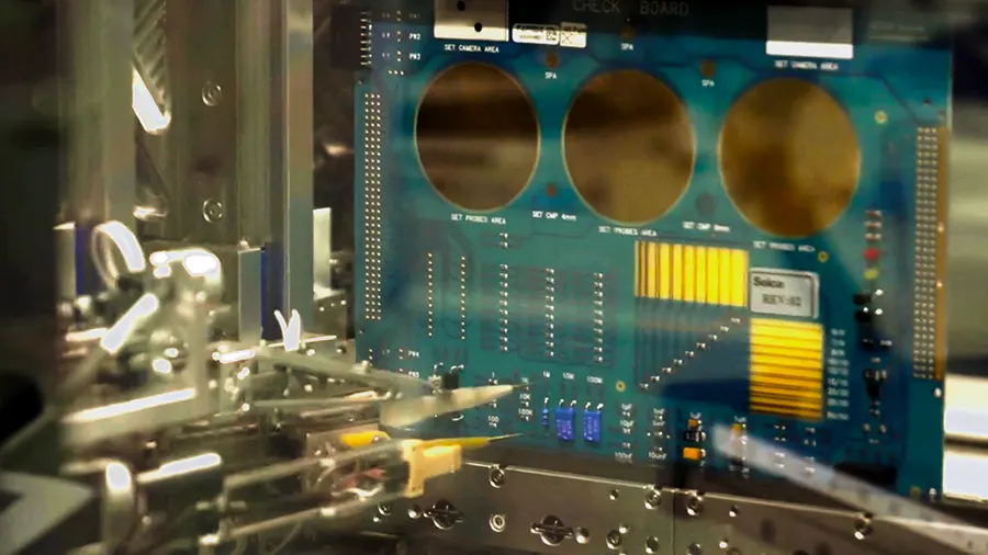
Electrical Testing Electrical testing is mandatory for all boards. This is the only way for any PCB manufacturer to ensure the product shipped has zero shorts or opens.
Visual inspection can never be 100% effective. Especially, if the defect is under the solder mask, electrical test is the only way to catch it.
Shipping Options FedEx, UPS, Will Call. You can use your own FedEx/UPS account number. International shipments allowed. All duties/customs are the responsibility of the customer. See shipping charges here.
Payment Terms Credit card (purchase order allowed only for select customers who have set up credit terms).
Additional Requirements For 4-layer or more orders, please include stack-up information. Please be available to clarify any discrepancies by providing your 24-hour contact number. IMPORTANT NOTE: 1. Web PCBs are manufactured to IPC-6012 Class 2 – No Coupon specifications. (Note that we do not provide any microsection reports or IPC coupons in Web PCB service. If you need such reports or you need your boards made to mil-spec or Class 3 specs, please ask for a custom quote). 2. Also, if your design has ITAR considerations, do mark the ITAR radio-button when getting a quote.
Restrictions (For some special boards, instant pricing is not available. We will send you custom quote instead.) For PCBs, special features like milling, blind/buried vias, mixed copper layers, etc., cannot be instantly priced online. However, please use the online price matrix anyway and press the CLICK HERE link. A Web Product Specialist will contact you and get you a quote as needed. For assembly, our online labor quote is for RIGID boards only with the below specifications: Minimum passive component size allowed is 0201. Minimum pitch allowed is 0.4 mm for regular SMT devices (for BGA the minimum pitch allowed is 0.5 mm). Maximum number of through-hole components (per board) is 20. Minimum component pad size must be 8 mil X 8 mil or 8 mil diameter. Furthermore, it does not include the following: 1. Assembly of flex or rigid-flex boards 2. Assembly of special items like PEM nuts, turrets terminals, rivets, and press-fit connectors. 3. Special assembly processes like: wire-bonding , conformal coating, underfills, staking, POP assembly, wires & cables assembly. 4. Assembly rework like cutting traces, soldering wire jumpers & cables onto the boards. If any of these is required, such services will be quoted separately by a Web Product Specialist.
OUR RIGHT TO REFUSE AN ORDER Sierra Circuits reserves the right to refuse any Web PCB order within 1 business day. This rarely ever happens, but may happen if the board design has special complexities that are not commensurate with the price paid online.
LEARN PCB
PCB Manufacturing
PCB Assembly
PCB Design and Layout
PCB Basics
Vias, Drilling & Throughplating
Mechanics
Surface
SMD
Quality
SPECIFICATIONS
PCB Fabrication
STANDARDS & POLICY
PCB Ordering
Policy

Sierra Circuits is
headquartered in Silicon Valley.
We welcome visitors at
our 70,000 sqft facility,
located at 1108 West Evelyn Avenue
in Sunnyvale, California.
Book a tour with an account manager today!
Let us introduce you to one of the most innovative communities of engineers and designers in the world.
We can help you plan your project from design to assembled board.

Manufacturing Equipment at Sierra Circuits

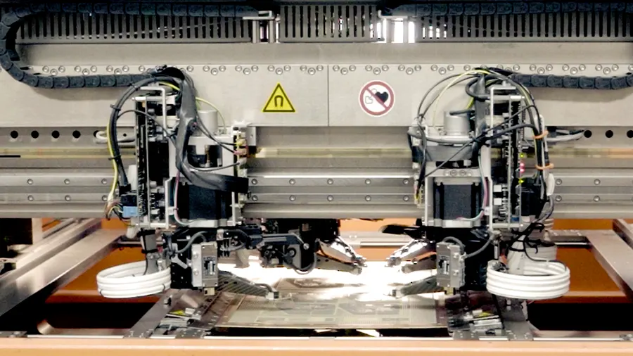
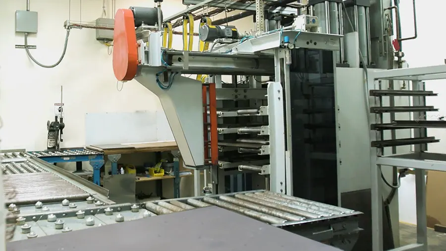
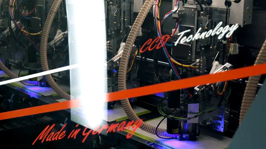
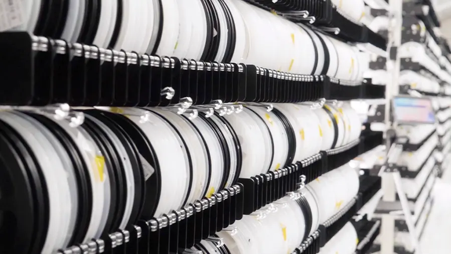
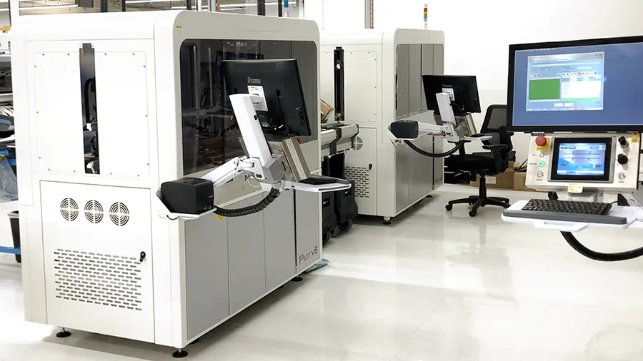
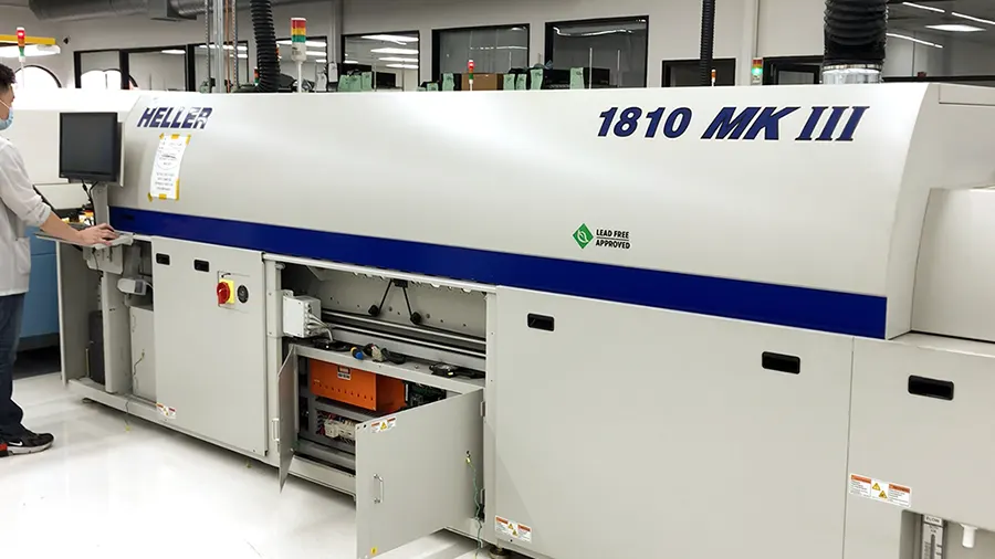
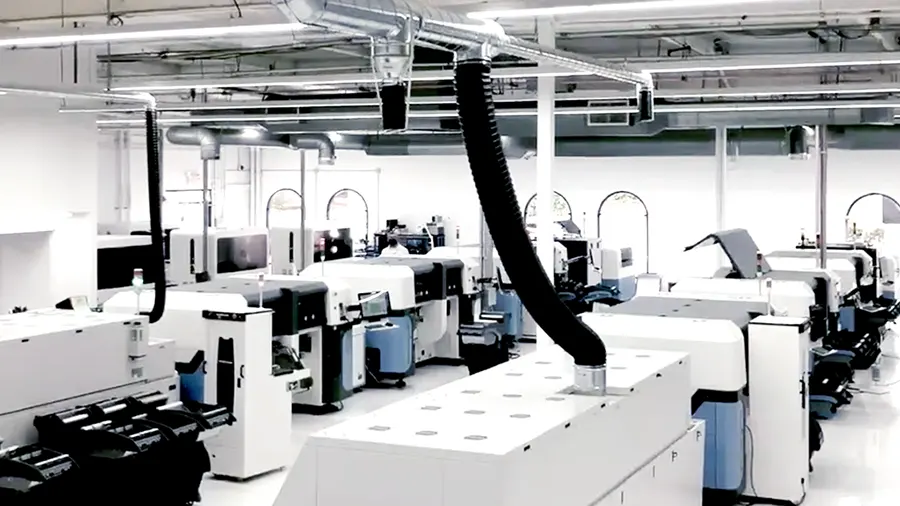
Our 70,000 sqft state-of-the-art campus in the heart of Silicon Valley contains the most advanced equipment required for the manufacture and assembly of your PCBs. Whether you’re looking for standard quick turn PCBs or boards with the tightest tolerances, made from exotic metals, there’s a reason Sierra Circuits leads the industry in quality and performance.

PCBs manufactured and assembled in the United States

Turn-times as fast as 1 day.

Sierra Circuits can manufacture your PCB and have it expedited to you within 24 hours.

Full turnkey boards, with assembly and components in as fast as 5 days.

Get an Instant, Itemized Quote

Talk to a Sierra Circuits PCB Expert today

24 hours a day, 7 days a week.

Call us: +1 (800) 763-7503
Book a Meeting with a Sales Rep
Email us: through our Customer Care form