Rigid PCB Specs


The Pitch

  • Manufactured in Silicon Valley
  • On-site inventory of the finest materials, up to 30 layers
  • 1-day turn-times available

The Parameters

  • Up to 30 layers
  • Board thickness: .005″ – .250″
  • Max panel size: 21″ x 29″
  • Min trace and space: .002″
  • Solder mask feature tolerance: .001″
  • Blind & buried vias
Start an Online Quote
LEARN PCB
PCB Manufacturing
PCB Assembly
PCB Design and Layout
PCB Basics
Vias, Drilling & Throughplating
Mechanics
Surface
SMD
Quality
SPECIFICATIONS
PCB Fabrication
STANDARDS & POLICY
PCB Ordering
Policy
Via Capabilities
Blind Via Min Total Pad Size 4 mils (.102 mm) over drill size
Min Laser Drill Size 4 mils (.102 mm)
Mechanically Drilled Annular Ring 4 mils (.102 mm) over drill size
Dielectric Material Thickness 2 mils (.051 mm)
Capture Pad Size 4 mils (.102 mm) over drill size
Laser Aspect Ratio .75:1
Buried Via Min Total Pad Size 5 mils (.127 mm) over drill size
Min Drill Size 6 mils (.152 mm) – depending on aspect ration
Capture Pad Size 5 mils (.127 mm) over drill size
Laser Aspect Ratio .75:1
Through Hole Min Total Pad Size 5 mils (.127 mm) over drill size
Min Drill Size 6 mils (.152 mm)
Capture Pad Size 5 mils (.127 mm) over drill size
Max Layer Count 26+
Min Finish Thickness .01″ (.254 mm)
Min Trace Width (I/L) 3 mils (.076 mm)
Min Trace Width (O/L) 3 mils (.076 mm)
Min Space Width (I/L) 3 mils (.076 mm)
Min Space Width (O/L) 3 mils (.076 mm)
Max Lamination Cycles 4
Min Hole Size 6 mils (.152 mm)
Min Pitch .157″ (.4 mm)
Stacked Vias Yes
Staggered Vias Yes
Conductive Filled Vias Yes
Non-Conductive Filled Vias Yes
Copper Plate Shut Microvias Yes
Heat Sinks Yes
UL 94V-0 (On Select Materials) Yes
Quality Reports
Specifications IPC-6012, Class 1, 2, 3, & 3D Yes
IPC-6013, Class 1, 2 & 3 Yes
31032 MIL-PRF-55110 (On Selected Materials) Yes
Reports / Certificates Micro Section Yes
Solderability Yes
X-Ray Fluorescence Yes
Ionic Contamination Yes
Time Domain Reflectometry (TDR) Yes
First Article Inspection (FAI) Yes
Certificate of Compliance (C of C) Yes
Electrical Test Yes
Construction
Panel Sizes 14×26″ (36×66 cm), 21×25″ (53×64 cm), 21x 29″ (53×74 cm), 12×18″ (30×46 cm), 18×24″ (46×61 cm), 16×18″ (41×46 cm)
Min Board Thickness .007″ (.178 mm)
Max Board Thickness .25″ (6.4 mm)
Thickness Tolerance < 10%
Bow & Twist Tolerance < 7%
Min Core Thickness .002″ (0.51 mm)
Min Dielectric .002″ (.051 mm)
Min Starting Copper Foil Weight 9 micron (.009 mm)
Preferred Materials*
FR-4 Lead Free Isola 370 HR Yes
Ventec VT47 Yes
Nan Ya NPG-170 Yes
Polyimide Isola P95 Yes
Nelco N7000-2 HT Yes
Arlon 85N Yes
Highspeed FR/MW Applications Isola I-speed Yes
FR 408HRR Yes
Nelco N4000-13 Yes
Nelco N4800-20 Yes
Teflon Nelco N9000-13 RF Yes
Rogers RO3000 Series Yes
Rogers RT/DUROID Series Yes
Rogers ULTRALAM 2000 Yes
Ceramic Rogers RO4003 Yes
Rogers RO4350 Yes
Rogers TTM 3, 4, 6, 10, 10i Yes
Taconics CER-10 Yes
Taconics RF-35, RF-35A2 Yes
Taconics RF-60 Yes
Flex DuPont Pyralux AP Yes
DuPont Pyralux LF Yes
DuPont Pyralux FR Yes
Laird IMPCB Yes
Drill
Smallest Laser Drill Diameter .003″ (.076 mm)
Largest Laser Drill Diameter .010″ (.254 mm)
Max Laser Aspect Ratio >.75:1
Min Mechanical Diameter .005″ (.127 mm)
Max Mechanical Aspect Ratio > 10:1
Min Mechanical Drill to Copper .005″ (.127 mm)
Min Plated Through Hole Tolerance +/- .002” (.051 mm)
Min Non Plated Through Hole Tolerance +/- .001” (.025 mm)
Pad Diameter
Rigid Inner Layer Drill + .008″ (.203 mm) + Class 2
Outer Layer Drill + .006″ (.152 mm) + Class 2
Flex Inner Layer Drill + .010″ (.254 mm) + Class 2
Outer Layer Drill + .008″ (.203 mm) + Class 2
Conductors
Pad Size Min Pad Size For Electrical Test .004″ (.102 mm)
Min Wire Bond Pad Size .004″ (.102 mm)
Min Trace Vs Copper Thickness Note: Thickness includes starting foil plus panel plates (for wrap if any) to beetched. 5 microns .002″ (.051 mm)
9 microns .0025″ (.064 mm)
3/8 oz .003″ (.076 mm)
1/2 oz .0035″ (.089 mm)
1 oz .0045″ (.114 mm)
2 oz .006″ (.152 mm)
3 oz .0065″ (.165 mm)
> 3 oz Contact Us
Min Space Vs Copper Thickness Note: Thickness includes starting foil plus panel plates (for wrap if any) to beetched. 5 microns .0025″ (.064 mm)
9 microns .003″ (.076 mm)
3/8 oz .0035″ (.089 mm)
1/2 oz .004″ (.102 mm)
1 oz .005″ (.126 mm)
2 oz .0065″ (.165 mm)
3 oz .007″ (.178 mm)
> 3 oz Contact Us
Permanent Solder Mask
Liquid Photoimageable (LPI) Colors Green, Red, Blue, Yellow
Gloss Semi-Gloss, Matte (Only In Green)
Min Dam/Web Size SMT .004″ (.102 mm)
Min Dam/Web Size BGA .0035″ (0.89 mm)
Clearance >.0005″ (.013 mm)
Mask-Defined SMT Or BGA (Not Ground Plane) Yes
Mask-Defined Features On Ground Plane Yes
Laser Direct Imaging (LDI) Colors Green, Black, Red, Blue
Gloss Semi-Gloss
Min Web for SMT .004″ (.102 mm)
Min Web for BGA .0035″ (.089 mm)
Clearance .005″ (.126 mm)
Mask-Defined SMT Or BGA (Not Ground Plane) Yes
Legend
Sprint Color White
Min Line .050″ (1.27 mm)
Min Heigth .025″ (.635 mm)
Screen Printable Colors White, Yellow, Black, Red
Min Line .007″ (.178 mm)
Min Heigth .030″ (.762 mm)
Surface Finishes
HASL (Vertical & Horizontal) Yes
Lead Free HASL Yes
OSP (Shikoku F2 & Entek) Yes
ENIG (Electroless Nickel / Immersion Gold) Yes
ENEPIG (Electroless Nickel-Electroless Paladium-Immersion Gold) Yes
Immersion Silver Yes
Tin Nickel Yes
Electrolytic Soft Gold Yes
Electrolytic Hard Gold Yes
Fabrication
Mechanical Min Route Cutter Available .021″ (.533 mm)
Routed Part Size Tolerance <.010″ (.254 mm)
Counter Sink Yes
Counter Bore Yes
Bevel Angles 20, 30, 45
Laser Milling, Depth Tolerance +/- .003″ (.076 mm)
Laser Routed Thickness <.032″ (.813 mm) Thick
Routed Array Yes
V Score Angles 30, 45, 60
Edge to Copper .007″ (.178 mm)
Dicing Edge to Copper .005″ (.127 mm)
Edge / Castellation Min Drill Via .010″ (.254 mm)
Edge Plating Yes
Other Screenable Materials
Carbon Ink Yes
Peelable Solder Mask Yes
Electrical Test
Controlled Impedance 5% w/ F/A
Hi Pot Yes
Test Voltage 40, 250, 500
Isolation Resistance (Mohms) >100
Continuity Resistance (Ohms) <.010
Min Pad Size .004″ (.102 mm)
LEARN PCB
PCB Manufacturing
PCB Assembly
PCB Design and Layout
PCB Basics
Vias, Drilling & Throughplating
Mechanics
Surface
SMD
Quality
SPECIFICATIONS
PCB Fabrication
STANDARDS & POLICY
PCB Ordering
Policy

Sierra Circuits is
headquartered in Silicon Valley.
We welcome visitors at
our 70,000 sqft facility,
located at 1108 West Evelyn Avenue
in Sunnyvale, California.
Book a tour with an account manager today!
Let us introduce you to one of the most innovative communities of engineers and designers in the world.
We can help you plan your project from design to assembled board.

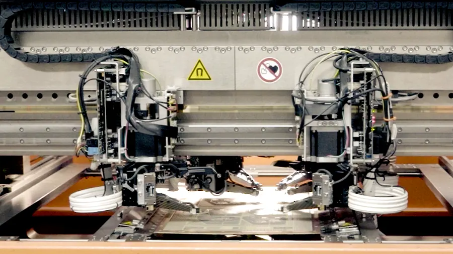
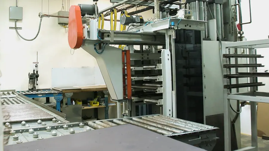
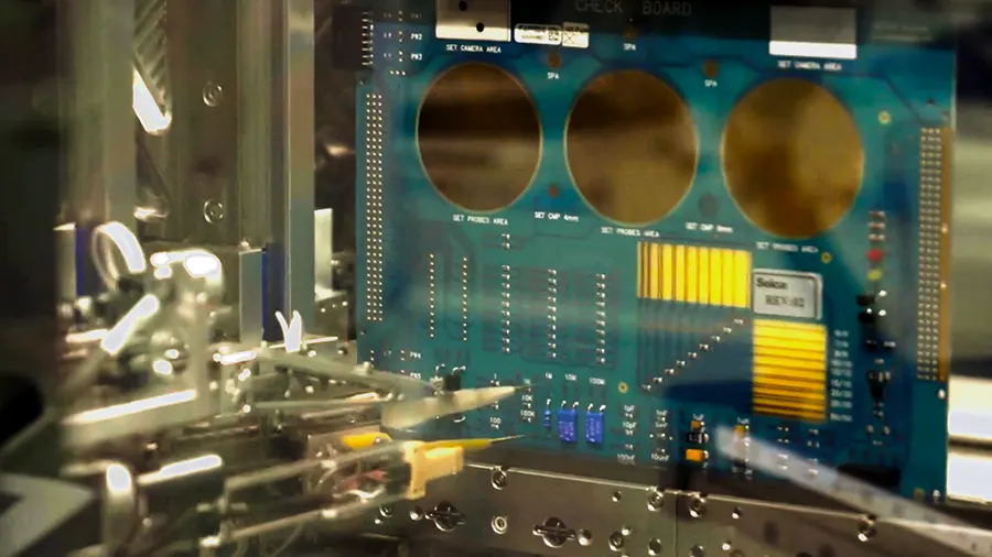
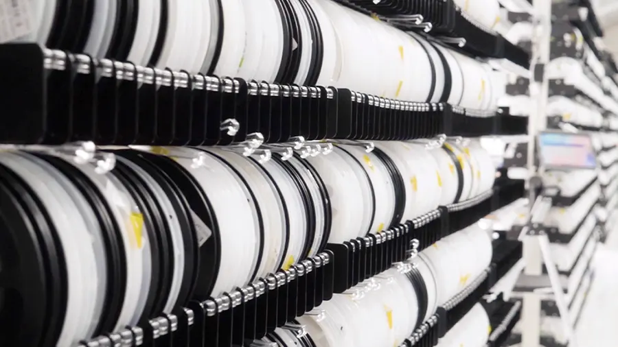
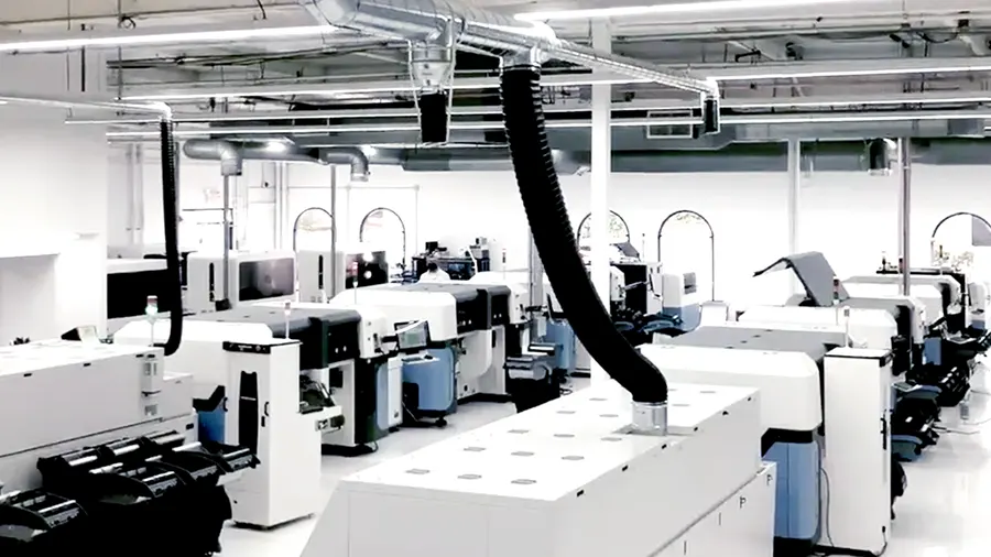
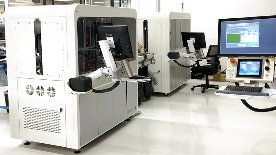
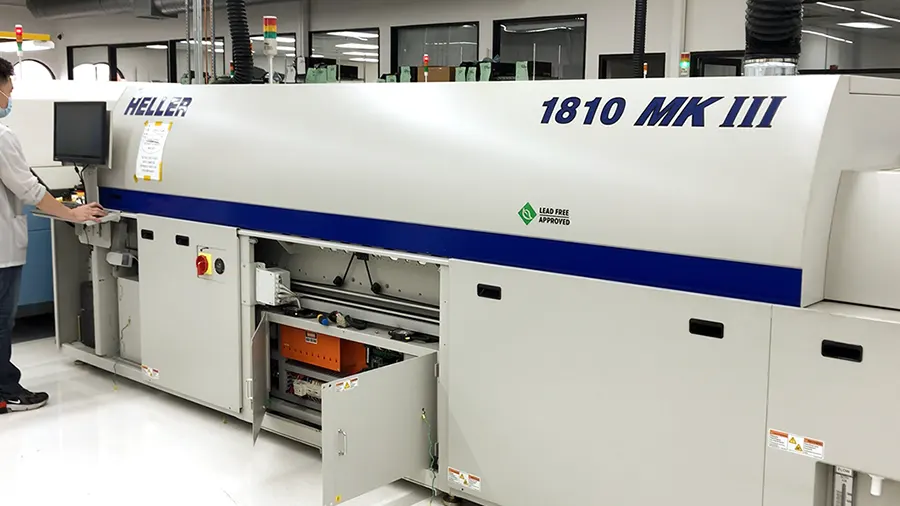
Manufacturing Equipment at Sierra Circuits

Our 70,000 sqft state-of-the-art campus in the heart of Silicon Valley contains the most advanced equipment required for the manufacture and assembly of your PCBs. Whether you’re looking for standard quick turn PCBs or boards with the tightest tolerances, made from exotic metals, there’s a reason Sierra Circuits leads the industry in quality and performance.

PCBs manufactured and assembled in the United States

Turn-times as fast as 1 day.

Sierra Circuits can manufacture your PCB and have it expedited to you within 24 hours.

Full turnkey boards, with assembly and components in as fast as 5 days.

Get an Instant, Itemized Quote

Talk to a Sierra Circuits PCB Expert today

24 hours a day, 7 days a week.

Call us: +1 (800) 763-7503
Book a Meeting with a Sales Rep
Email us: through our Customer Care form