Selecting the right material, whether PTFE or non-PTFE, is crucial for your RF designs. This choice significantly affects signal loss, dimensional stability, and board reliability. It’s not just a simple decision; it depends on the specific needs of your applications.
PTFE and ceramic-filled PTFE laminates offer superior electrical performance and are preferred for radio-frequency applications.
On the other hand, non-PTFE materials strike a balance between high-speed signal transmission and hassle-free fabrication.
In our recent webinar, choosing the right material for your RF PCB designs, we surveyed our attendees about their go-to RF material choice. Here are the results:

You’ll learn about PTFE and non-PTFE materials’ characteristics in this article. As an RF engineer, knowing these details will help you make an informed decision while choosing high-frequency laminates.
What are PTFE materials?
PTFE-based materials are composite laminates. They are made of polytetrafluoroethylene (PTFE), additives, and fillers. These fillers enhance the laminates’ electrical, mechanical, and thermal properties.
Key components of polytetrafluoroethylene laminates
1. PTFE matrix
The PTFE matrix forms the fundamental structure of the laminates. Polytetrafluoroethylene is a synthetic fluoropolymer known for its non-stick properties.
It is the base polymer that provides minimal signal loss and excellent thermal stability. Its high resistance to solvents, chemicals, and moisture makes it suitable for harsh operating conditions.
2. Additives and fillers
By carefully selecting the additives and fillers, you can tailor PTFE-based materials to meet your specific requirements.
Additives and fillers can be categorized into two main types:
- Reinforcements: Reinforcements are added to increase the laminate’s mechanical strength and dimensional stability. Standard reinforcements include:
- Glass fibers: These provide stiffness and strength to the material, improving its tensile strength and impact resistance.
- Aramid fibers (e.g., Kevlar): They improve the material’s wear resistance, elastic modulus, and chemical resistance.
- Fillers: They are added to modify the RF laminate’s thermal and electrical properties.
- Ceramic fillers: These fillers lower the material’s dielectric constant and dissipation factor. They minimize signal losses.
- Metal particles: Adding metal particles can improve the thermal conductivity of RF PCB substrates.
To learn every step of designing a high-performing radio-frequency board, download our eBook.
RF & Microwave Design Guide
8 Chapters - 44 Pages - 60 Minute ReadWhat's Inside:
- Basics of RF and microwave board design
- Choosing RF materials
- Trace, grounding, via, and stack-up design
- Component selection and placement
- Testing and isolation requirements to avoid interference
Download Now
5 important characteristics of PTFE laminates
- Low dielectric constant (Dk): Dk measures a material’s ability to store electrical energy. The lower the Dk, the lesser the signal loss. PTFE offers Dk values as low as 2.2, significantly lower than the standard FR4 PCB material (around 4.5).
- Low dielectric loss: Dielectric loss measures the energy dissipation within the material when subjected to an electric field. PTFE exhibits lower dielectric loss, ensuring efficient high-frequency signal transmission. This characteristic is crucial for maintaining signal strength in radio frequency applications.
- Excellent thermal stability: These laminates have a low coefficient of thermal expansion ( 50-135 ppm/°C). This limits the expansion and contraction of the material with temperature fluctuations.
- Chemical resistance: They are highly inert, offering excellent resistance to solvents, acids, and bases. This property enhances the durability and reliability of RF applications, especially in harsh environments where chemical exposure is a concern.
- RoHS compliance: PTFE materials are typically RoHS compliant; they do not contain harmful substances like lead, mercury, cadmium, and flame retardants.
4 challenges in fabricating PTFE substrates
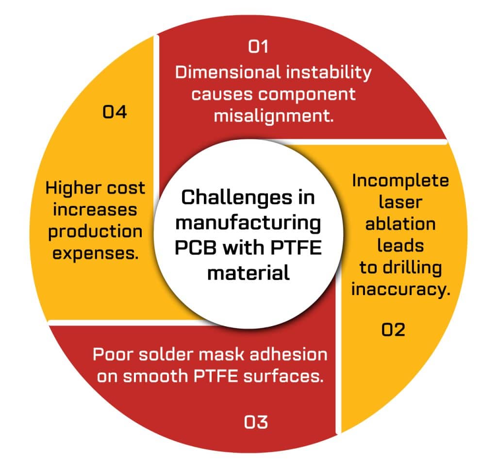
While PTFE materials offer numerous advantages for RF applications, they also present challenges that designers and manufacturers must address. These include:
1. Dimensional instability causes component misalignment
PTFE is a relatively soft and flexible material compared to many other substrates. Its softness can cause issues during drilling, routing, and milling. The material may deform under the pressure of cutting tools.
Due to its flexibility, PTFE is prone to dimensional instability during machining. This can result in component misalignment.
2. Incomplete laser ablation leads to drilling inaccuracy
Since PTFE is UV transparent, it does not absorb the UV laser energy effectively. This lack of absorption causes the laser energy to pass through the material. As a result, the energy is not converted into heat needed to vaporize the material, making the ablation process ineffective.

Advances in laser technology provide solutions to inefficient drilling. Carbon dioxide lasers help achieve the correct drilling registration with PTFE materials.
This laser ablation technique uses gas as the lasing medium and can create 50-70 μm diameter holes. CO2 lasers can only ablate dielectric materials (not copper) with high reflectivity from metal surfaces.
At Sierra Circuits, we use advanced CO2 laser drilling machines for PTFE materials.
3. Poor solder mask adhesion
PTFE is chemically inert and has a low surface energy. The smooth surface can hinder the mechanical interlocking of the solder mask. Its high CTE might cause mechanical stress between the solder mask and the substrate during thermal cycling.
Exposing a PTFE surface to plasma treatment can increase surface roughness and activate it, improving solder mask adhesion.
4. High material cost increases production expenses
Since PTFE materials cost more, it significantly increases manufacturing expenses. These materials require specific handling and processing techniques that differ from those used for non-PTFE. The specialized processes involve sophisticated equipment and stringent quality control measures, contributing to higher manufacturing costs.
What are ceramic-based PTFE laminates?
These are high-performance substrates composed of polytetrafluoroethylene reinforced with ceramic particles.
Glass fiber weaves can cause undesired skew and incorrect phase response. In contrast, ceramic-filled laminates eliminate these issues, making them ideal for RF systems.
Ceramics can be engineered for specific material properties, providing:
- Improved mechanical strength: Ceramic fillers can enhance the stiffness and hardness of laminates.
- Enhanced wear resistance: They improve the wear resistance of PTFE materials, making them more suitable for applications where friction and abrasion are concerns.
- Higher thermal conductivity: Ceramic-filled PTFEs incorporate a low CTE, improving their thermal stability and allowing them to withstand higher temperatures.
- Chemical resistance: Ceramics can enhance the chemical resistance of PTFE materials and allow exposure to harsh chemicals and solvents.
- Cost-effectiveness: Depending on the specific application and requirements, using ceramic fillers in PTFE-based materials can offer a cost-effective solution while enhancing electrical and mechanical performance.
Sierra Circuits fabricates high-quality RF and microwave PCB prototypes. Visit our RF and microwave PCB manufacturing capabilities to learn more.
What are non-PTFE materials?
These are the substrates made from materials other than polytetrafluoroethylene. Common examples include FR-4 and polyimide materials.
Key characteristics include:
- Varied dielectric constants: The wide range of dielectric constants (typically between 3.0 and 10.0) provides design flexibility for different frequency ranges.
- Cost-effectiveness: Generally more affordable than PTFE, making them suitable for cost-sensitive applications.
- Easier to fabricate: Easier to process and fabricate than PTFE and requires less production time.
Disadvantages of non-PTFE laminates
- Non-PTFE materials generally have a higher dielectric constant than PTFE. This can lead to increased signal loss at higher frequencies.
- The higher dissipation factor results in greater signal attenuation.
- Non-PTFE materials may have lower thermal stability and higher CTE than PTFE. Lower thermal stability can lead to material degradation and mechanical failures. Higher CTE can also contribute to dimensional changes and potential stress on solder joints over time, affecting long-term reliability.
For tips on selecting materials for your radio-frequency PCBs, see how to pick RF PCB materials: 6 important factors to consider.
Non-PTFE Vs. PTFE Vs. ceramic-filled PTFE radio-frequency materials
Here’s a quick comparison among non-PTFE, PTFE, and ceramic-filled PTFE materials:
| Parameters | Non-PTFE | PTFE | Ceramic-filled PTFE |
|---|---|---|---|
| Cost | Moderate to low | High to very high | High to very high |
| Fabrication complexity | Low to moderate | High to very high | High to very high |
| Glass transition temperature (Tg) | 130°C to 280°C | -60°C to 200°C | 150°C to 220°C |
| Coefficient of thermal expansion (CTE) | 10-50 ppm/°C | 50-200 ppm/°C | 30-80 ppm/°C |
| Dielectric constant (Dk) | 3.5 - 4.5 | 2.1 - 2.6 | 3.0 - 10.0 |
| Loss tangent (Df) | 0.002 - 0.02 | 0.0001 - 0.002 | 0.001 - 0.005 |
| Thermal conductivity | Moderate (0.3 - 0.5 W/m·K) | Low (0.2 - 0.3 W/m·K) | High (0.5 - 1.0 W/m·K) |
| Mechanical strength | High | Low | Moderate |
| Chemical resistance | Moderate to good | Excellent | Excellent |
| Moisture absorption | Moderate (0.1% - 0.5%) | Very low (<0.01%) | Low (0.02% - 0.1%) |
| Thermal stability | Moderate to good | Excellent | Excellent |
| Adhesion to Copper | Good | Challenging | Good |
| Applications | Consumer electronics | RF and microwave | RF, microwave, and military |
Common non-PTFE, PTFE, and ceramic-filled PTFE laminates
Non-PTFE materials
| Isola | ||
|---|---|---|
| Material name | Dielectric constant (Dk) | Dissipation factor (Df) |
| FR408HR | 3.68 | 0.0095 at 10GHz |
| I-Tera® MT40 | 3.45 | 0.0031 at 10GHz |
| I-speed | 3.63 | 0.0060 at 10GHz |
| Panasonic | ||
|---|---|---|
| Material name | Dielectric constant (Dk) | Dissipation factor (Df) |
| R-5775K | 3.40 | 0.004 at 10GHz |
| R-5795(U) | 3.1 | 0.0012 at 14GHz |
PTFE-based materials
| Rogers Corporation | ||
|---|---|---|
| Material name | Dielectric constant (Dk) | Dissipation factor (Df) |
| RT/duroid® 5880 | 2.20 ± 0.02 | 0.0009 at 10GHz |
| RT/duroid® 5870 | 2.33 ± 0.02 | 0.0012 at 10GHz |
| CuClad® 250 | 2.40 to 2.60 | 0.0018 at 10GHz |
| CuClad® 233 | 2.33 | 0.0013 at 10GHz |
| AGC | ||
|---|---|---|
| Material name | Dielectric constant (Dk) | Dissipation factor (Df) |
| TLY-5 | 2.20 ± 0.02 | 0.0009 at 10 GHz |
| TLX-8 | 2.55 ± 0.04 | 0.0018 at 10 GHz |
Ceramic-filled PTFE materials
| Rogers Corporation | ||||
|---|---|---|---|---|
| Material name | Dielectric constant (Dk) | Dissipation factor (Df) | ||
| RO3003™ | 3.00 +/- .04 | 0.0010 at 10GHz | ||
| RO3010™ | 10.2 +/- .30 | 0.0022 at 10GHz | ||
| CLTE-XT | 2.93 | 0.0010 at 10GHz | ||
| CLTE-MW | 3.03 to 3.10 | 0.0015 at 10GHz | ||
| AGC | ||
|---|---|---|
| Material name | Dielectric constant (Dk) | Dissipation factor (Df) |
| RF-30A | 2.97 +/- 0.05 | 0.002 at 10GHz |
| TSM-DS3M | 2.94 +/- 0.04 | 0.0011 at 10GHz |
| Ventec international group | ||
|---|---|---|
| Material name | Dielectric constant (Dk) | Dissipation factor (Df |
| VT-3703 | 3.0±0.04 | 0.0009 at 10GHz |
| VT-3706 | 6.15±0.05 | 0.0019 at 10GHz |
PTFE and non-PTFE laminates each have their own set of challenges and advantages. Analyze them with the help of your manufacturer to make the right choice for your RF designs.
Pick the best materials that suit your applications instantly with our advanced PCB Material Selector.