Via tenting in PCBs safeguards the plated holes from contamination. It resists seepage of dust, moisture, and solder paste into vias.
Or else it could lead to corrosion or short circuits.
Via tenting technique is beneficial in BGA and SMT areas, where the risk of short circuits is very high.
Here, you’ll learn 11 design rules for via tenting, essential fab notes to include, and different via tenting techniques.
What is PCB via tenting? Why is it used?
Via tenting covers the exposed portion of the via and annular ring with a solder mask or other insulating material, creating a tent-like shape over the opening.
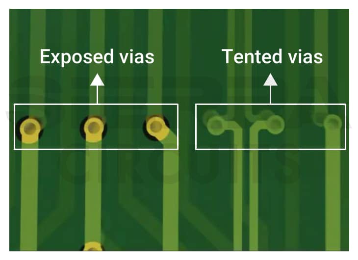
Via tenting is the simplest and most cost-effective method of protecting the plated holes.
To tent a via, simply remove the mask clearances from the vias you want to cover. No special measures are necessary to ensure the hole remains closed.
The tenting process is suitable for vias with a diameter of 12 mil or less. Vias larger than 15 mil in diameter may be too large for effective tenting.
The primary purpose of tented vias includes:
- Electrical isolation: It creates a protective barrier between the via and surrounding conductive elements, preventing unintended electrical contact. Additionally, hole tenting minimizes crosstalk in high-speed PCBs.
- Prevent solder wicking: It stops solder from being drawn into the via, a process known as solder wicking, which can cause short circuits and disrupt current flow.
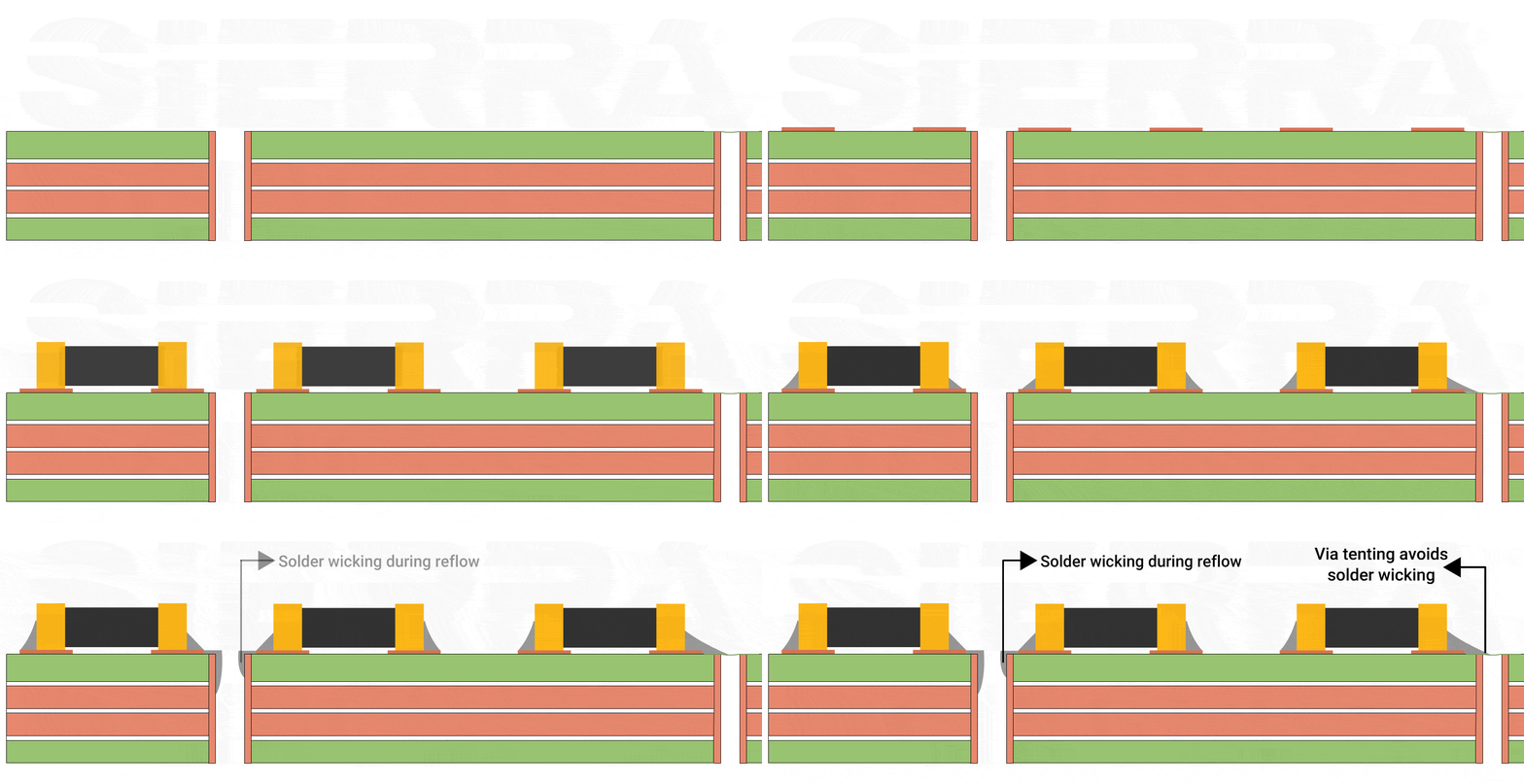
- Address assembly concerns: Tented vias avoid various assembly issues like flux residue and solder wicking.
- Environmental protection: In harsh environments (e.g., marine, industrial), tenting shields the copper within the via from corrosion and damage.
11 PCB design rules for via tenting
- Consider tenting vias based on the PCB design and via size. It’s generally easier to tent smaller vias, but vias larger than 15 mil in diameter may be too large for effective tenting.
- Position tented vias away from high-stress areas to avoid cracking or delamination of the tenting material.
- Make sure the thermal expansion characteristics of the tenting material and PCB substrate are similar to avoid tenting failures or cracked vias caused by excessive expansion or contraction.
- Avoid placing vias on edges or crowded areas to ensure efficient solder mask adhesion.
- Use a tenting material with dielectric properties closely matching the dielectric material to reduce impedance mismatches.
- Verify your PCB manufacturer’s capabilities in advance to ensure they offer via tenting services that meet your design requirements.
- Adhere to IPC guidelines for via size, spacing, and placement to improve the tenting process and ensure signal integrity.
- Tent both sides of the vias to protect them against oxidation and corrosion.
- Ensure the solder mask fully covers the via opening. Be aware that larger vias may have small air gaps under the tent that could slightly reduce the insulating effectiveness of the tenting. Therefore, confirm that via dimensions and aspect ratios are within acceptable limits.
- Indicate your via tenting requirements in your fab notes (readme.txt/Gerber). This note indicates that you have intentionally removed the mask clearances from some of your vias.
- Tent the vias under QFPs, especially near pins, to prevent short circuits from solder residue. Cover dogbone vias for BGAs to enhance performance.
For more design for manufacturing guidelines, download our DFM handbook.

Design for Manufacturing Handbook
10 Chapters - 40 Pages - 45 Minute ReadWhat's Inside:
- Annular rings: avoid drill breakouts
- Vias: optimize your design
- Trace width and space: follow the best practices
- Solder mask and silkscreen: get the must-knows
Download Now
Fabrication notes for tented vias
Provide these details to your PCB manufacturer for via tenting:
- All vias with a diameter of 0.305 mm [0.012 in] or less must undergo a tenting process on both sides.
- The combined height of the LPI solder mask and dry film solder mask must not exceed 0.076 mm [0.003 in] above the covered pad surface.
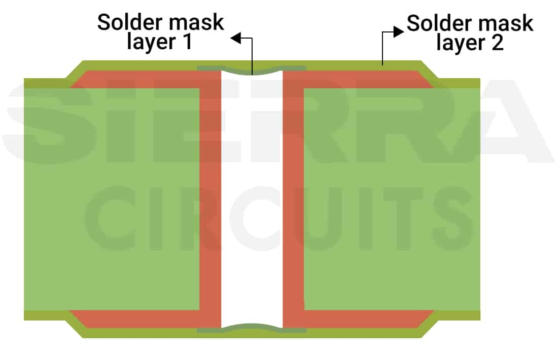
- Create a Type II-b tented and covered structure as per IPC-4761.
- The dry film solder mask must cover the via and not extend beyond the associated land.
- Use a conforming dry film solder mask as per IPC-SM-840, Class H.
- Confirm the tent height using a microsection evaluation of a representative quality conformance coupon.
At Sierra Circuits, we achieve flawless via tenting through precise solder mask application and alignment.
We use high-quality solder mask materials to ensure reliable via covering. To learn more, check out our PCB manufacturing services.
Tented via fabrication process
To tent vias, fabricators mainly use two materials: solder resist ink and dry film solder mask.
Via shielding using solder resist ink
Steps to tent vias with solder resist ink:
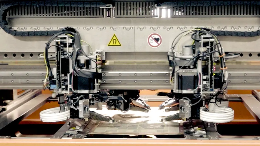
- The liquid solder mask is applied to the PCB surface using screen printing, spray coating, or curtain coating.
- The applied ink is cured with UV light or heat to harden and stick to the PCB.
- As the solder mask cures, it covers the via, creating a protective tent-like structure.
While this method is common and works well with traditional processes, it might not be suitable for smaller holes due to coverage issues. The thickness of the solder mask tent over the via can vary based on PCB design requirements and the type of solder mask used, typically ranging from 0.05 mm to 0.1 mm.
Hole protection using dry film solder mask
Dry film solder mask tenting is suitable, especially for high-density PCBs with small via sizes.
The process of dry film solder mask tenting includes the following steps:
- A photosensitive dry film is pressed directly onto the board to cover the via on PCBs.
- The applied dry film is exposed to UV light using a photomask and then developed to remove the unexposed areas, creating a tent-shaped structure over the via holes.
- The dry film then undergoes a heat treatment to improve its adhesion and durability.
Dry film solder mask tenting has advantages over solder resist tenting, such as better adaptation to small via sizes and improved control over thickness. However, it has some drawbacks, including higher costs and more intricate processing requirements.
Via covering techniques
PCB via tenting is crucial in optimizing electrical performance and heat dissipation and ensuring component reliability. Depending on the design requirements, vias can be fully or partially covered or left entirely exposed.
Exposed vias, for instance, leave the via hole and annular ring uncovered, making them ideal for high-current traces. However, they also come with drawbacks, such as an increased risk of tarnishing, corrosion, and potential shorts, especially during soldering and testing.
Understanding each of these tenting techniques helps you in selecting the best option based on your requirements.
| Tenting techniques | Description | Advantages |
|---|---|---|
| Full tenting | Covers both the annular ring and the via hole on both sides of the PCB. |
|
| Partial tenting | Shields the annular ring, but the via hole remains exposed on both sides. |
|
| Single-sided tenting | Protects only one side of the PCB, typically the component side. |
|
The choice between full, partial, or single-sided tenting can also depend on the via size and shape. For example, large vias may benefit from partial tenting to reduce the risk of trapped fluids.
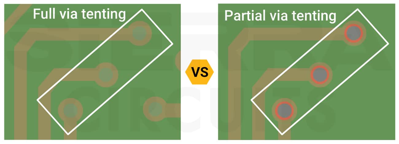
Via tenting types
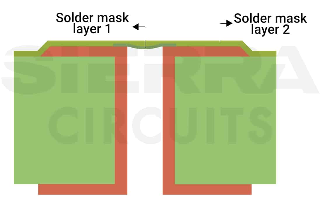
Via covering and filling benchmarks are depicted by IPC-4761 standards. In this section, you will learn 4 types of via tenting.
Type I(a): Via is tented on a single side using a solder mask. There is no protection for the hole walls on the other side. It can also have long-term reliability issues.
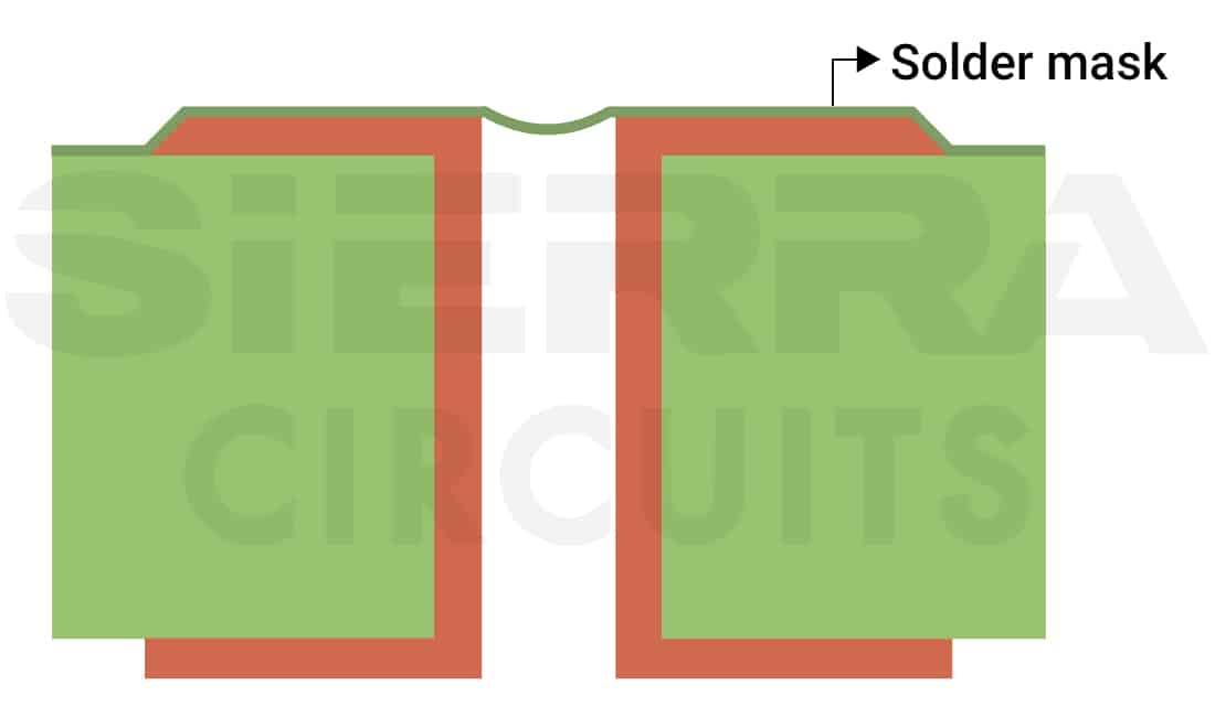
Type I (b): Solder mask covers the hole on both sides. This type of via covering can have dimples on the surface.

Type II (a): Here, 2 solder mask layers cover the via on a single side.
Type II (b): The via is tented and covered with a secondary mask on both sides.
To know more about other via protection techniques, read via filling techniques designers need to know for PCB fabrication.
8 benefits of via covering
- Tenting vias protect them from physical damage, oxidation, contamination, and electrical shorts. When designing PCBs with through-hole components for wave soldering, it’s essential to tent vias to prevent the solder from causing short circuits.
- Covered vias help to avoid complete exposure of pads beneath BGA, lowering the chance of short circuits caused by excessive solder flow.
- Tented vias are also crucial near SMT pads to prevent solder paste from creating suboptimal solder joints and solder bridges between that via and the surface mount pad.
- Covered vias ensure the legibility of silkscreen text.
- Tented vias reduce electromagnetic interference between nearby signal traces.
- Via tenting is a cost-effective method to safeguard the vias and the surrounding copper. A liquid photo-imageable solder mask is the most economical option.
- Tenting helps in PCB thermal management by reducing the impact of air gaps around vias. Covering the vias allows you to control better and predict heat dissipation, preventing hot spots and improving overall thermal performance.
- Tenting vias can help prevent solder bridging during assembly by blocking solder flow into the via. It also reduces the risk of paste migration from SMT pads, which can happen when you drill vias near the edges of SMT pads or in standard BGA “dog-bone” designs.
Tenting vias offer numerous benefits from different viewpoints, such as protecting from environmental factors, preventing solder wicking, offering electrical isolations, and cost efficiency. These advantages via covering as the preferred option for many PCB manufacturers and designers.
