Submitting the right design data to fab houses is crucial for ensuring the efficient production of your circuit board. PCB file formats such as IPC-2581, Gerber, and ODB++ offer comprehensive data packages that cater to different aspects of the manufacturing and assembly processes.
Here, you will learn 3 design data formats, from which you can choose the one that suits you the best. You will also learn the specific files you need to submit when requesting quotes for PCB fabrication and assembly services.
What files do PCB manufacturers need?
Fab houses require specific data that provide detailed information about your circuit board design and assembly.
- IPC-2581 (this is a unified data format that integrates all the files required to fabricate your board)
If you opt for Gerber/ODB++, you have to submit the following:
- Gerber/ODB++
- NC drill files:
- IPC-NC-349
- Excellon drill file
- IPC netlist
- Bill of materials (BOM)
- Pick and place files (centroid files)
- Fab drawings
- NC drill files:
IPC-2581
The IPC-2581, also known as IPC-DPMX (digital product model exchange), provides a unified design data format, enabling seamless data exchange between designers and fab houses.
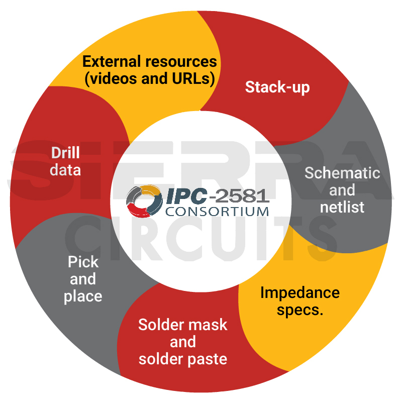
IPC-2581 checklist for fabrication
Here’s the list of files you need to submit to the manufacturer to get your board fabricated.
| File names | Description |
|---|---|
| Stack-up | Component top (for assembly), solder paste top, silkscreen top, solder mask top, all outer and internal signal/copper layers, solder mask bottom, silkscreen bottom, solder paste bottom, component bottom (for assembly), drill layers, routing layer. documentation (fab drawing in gerber format) |
| Netlist | Ensure the netlist accurately reflects the connectivity of all components and traces on the PCB. |
| Component Information | Include component names, values, datasheets, and BOM references for fabrication clarity. |
| Footprint Library | Provide an extensive library of component footprints for precise fabrication placement. |
| Fabrication Drawings and Instructions | Provide detailed drawings for fabrication, including drill drawings, solder mask, and paste mask. |
| Special Fabrication Instructions | Provide specific instructions for solder mask, paste mask, and any additional fabrication processes. |
Sierra Circuits fabricates best-in-class circuit boards within a quick turnaround time. Visit our PCB manufacturing capabilities to learn more.
IPC-2581 checklist for assembly
Make sure you submit these files if you opt for assembly services.
| File names | Description |
|---|---|
| Netlists (IPC-D-350 and IPC-D-356) | Provide information about the electrical connectivity of the board, ensuring correct assembly |
| Centroid File (Pick-and-place files for automated assembly) | Contains the X-Y coordinates, rotation, and side of each component, essential for automated assembly |
| BOM | Lists all components, part numbers, and quantities |
| Testpoint reports | Useful for quality control and verifying electrical functionality |
| Bottom silkscreen | Provides additional marking information for assembly |
The assembly data remains the same, irrespective of the file format you choose.
Sample list of IPC-2581 design data
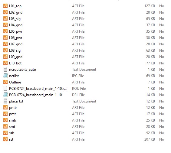
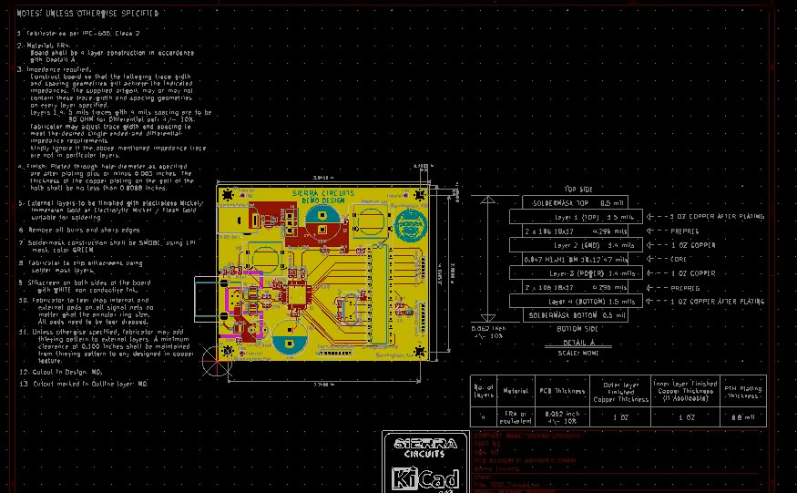
Things to include in your IPC-2581 fab drawings:
-
- Class of the PCB (class 1, class 2, or class 3)
- Stack-up details
- Overall board thickness
- Solder mask details
- Silkscreen specifications
- Layer-wise impedance details
- Cut-out details
- Drill chart
- Version number and date
Gerber files
Gerber files are the most widely used format for PCB manufacturing. These files drive the photoplotter to create the film needed to expose each conductor layer.
They are limited to 2D representations and do not include information about design rules, net connectivity, or component libraries. Gerber files enable manufacturing equipment to accurately place copper, solder mask, and silkscreen layers.
There are two primary versions of the Gerber format:
1. Standard Gerber (RS-274-D): This version is now obsolete.
2. Extended Gerber (RS-274X): This format is currently in use. It includes meta-data about the files, such as file attributes, and this format is known as X2.
The standard file extension of Gerber files is “.GBR” or “.GB”.
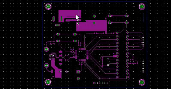
Gerber checklist for fabrication
| File names | Description |
|---|---|
| Stack-up | Defines the circuit board layer order |
| Excellon drill file | Contains tool codes and X-Y coordinates of all holes in either ASCII or EIA format, crucial for precision drilling |
| Drill tool list | Lists the tools needed for drilling operations. Sometimes, this will be integrated in the drill file/NC file |
| Top, bottom, and internal copper layers | These layers define the conductive traces on the board. It should be provided in positive polarity |
| Top and bottom solder mask | Contains the data related to solder mask layers |
| Top and bottom silkscreen layers | Includes reference designators and other markings |
| Board outline & milling layer | Comprises of dimensions, cutouts, chamfers, radii, bevels, and scores necessary for defining the board's shape |
| Aperture/D-Code list | Necessary for interpreting Gerber files if the set is not RS-274X compliant |
| Solder paste application areas | Defines areas for applying solder paste to create stencils. |
| DXF/DWG files for PCB Layout | Additional CAD data for reference. |
| Specical instructions, if any | This may include guidelines such as: No layers are mirrored.. |
Gerber checklist for assembly
| File names | Description |
|---|---|
| Netlists (IPC-D-350 and IPC-D-356) | Provide information about the electrical connectivity of the board, ensuring correct assembly |
| Centroid File (Pick-and-place files for automated assembly) | Contains the X-Y coordinates, rotation, and side of each component, essential for automated assembly |
| BOM | Lists all components, part numbers, and quantities |
| Testpoint reports | Useful for quality control and verifying electrical functionality |
| Bottom silkscreen | Provides additional marking information for assembly |
Things to include in your Gerber fab drawings:
- PCB materials to be used
- Holes count and corresponding sizes
- PTH/NPTH segregation
- Surface finish
- Drill guides
- Secondary drill needs
- Annular ring dimensions
- Panelization requirements
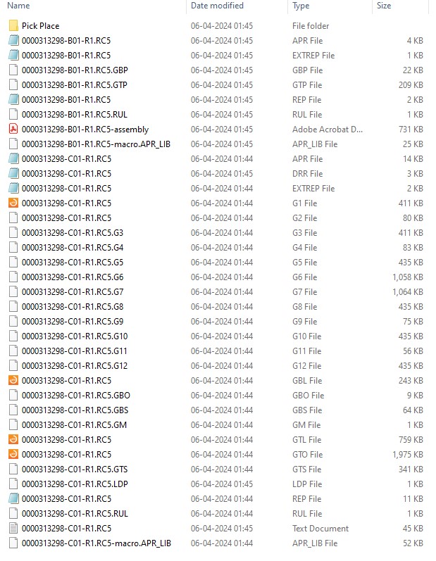
Sample list of Gerber files
Design for Manufacturing Handbook
10 Chapters - 40 Pages - 45 Minute ReadWhat's Inside:
- Annular rings: avoid drill breakouts
- Vias: optimize your design
- Trace width and space: follow the best practices
- Solder mask and silkscreen: get the must-knows
Download Now
ODB++
ODB++ deals with CAD to CAM data exchange. When ODB++ is used, its data is stored in multiple files, and the folders are arranged hierarchically. The designers will use common operating system commands that retain the hierarchy structure by fusing all of the data into one compressed file.
This format permits the storage of volumes of data in a single file that comprises stack-up, BOM, component placement coordinates, and dimension & fabrication details. ODB++ can be accessed through EDA tools, making it almost a universal format throughout board manufacturing.
Difference between Gerber and ODB++
Gerber RS274X is a frequently used format for board design. It is a single file with layer information, pad shapes, drawings, etc. A Gerber cannot define the layer stack-up and the drill files, whereas the ODB++ format can define such kind of data.
ODB++ checklist for fabrication
| ODB++ design data | File information |
|---|---|
| Image data | Features board files, including lines, pads, arcs, polygons, islands, holes with attributes, and unique identifiers |
| Component information | Component placement files (x/y location, rotation), linked to EDA/data file. The data includes part height, mounting style, and assembly surface (top/bottom) |
| EDA/data | Includes physical and hierarchical trace properites |
| CAD netlist | Defines testing requirements for vias and pads as per IPC-D-356B |
| Drill information | Provides the drill data for through-hole drilling or blind/buried vias. Differentiates vias, plated (PTH), and non-plated through-holes (NTH) |
| Routing information | Describes board cut-out description, including inner cut-outs. Single routing layer with lines, arcs, and pads |
| Stack-up | Defines the layer order of component top (for assembly), solder paste top, silkscreen top, solder mask top, all outer and internal signal/copper layers, solder mask bottom, silkscreen bottom, solder paste bottom, component bottom (for assembly), drill layers, routing layer. documentation (fab drawing in gerber format) |
ODB++ checklist for assembly
| File names | Description |
|---|---|
| Netlists (IPC-D-350 and IPC-D-356) | Provide information about the electrical connectivity of the board, ensuring correct assembly |
| Centroid File (Pick-and-place files for automated assembly) | Contains the X-Y coordinates, rotation, and side of each component, essential for automated assembly |
| BOM | Lists all components, part numbers, and quantities |
| Testpoint reports | Useful for quality control and verifying electrical functionality |
| Bottom silkscreen | Provides additional marking information for assembly |
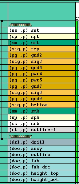
Sample list of ODB++ files
Things to include in your ODB++ fab drawings:
- PCB materials to be used
- Holes count and corresponding sizes
- PTH/NPTH segregation
- Surface finish
- Drill guides
- Secondary drill needs
- Annular ring dimensions
- Panelization requirements
