No-Touch PCBs Specs


The Pitch

  • Automated and simple process for PCB Fabrication
  • Manage your own design and manufacturability
  • Quality bare boards manufactured in the USA

The Parameters

  • 2, 4, 6-layer boards
  • FR-4 material, 0.062” (1.57 mm) thick
  • HASL or ENIG finish
  • Green Solder Mask, White Legend
  • 4-mil trace/space available
  • Automated DFM before you order
Start an Online Quote
LEARN PCB
PCB Manufacturing
PCB Assembly
PCB Design and Layout
PCB Basics
Vias, Drilling & Throughplating
Mechanics
Surface
SMD
Quality
SPECIFICATIONS
PCB Fabrication
STANDARDS & POLICY
PCB Ordering
Policy
No Touch PCB Specifications
Layers 2, 4 and 6-layer boards made to IPC-600 Class 2 specs.
Data required Gerber files in RS-274X format only (Extended Gerber) or ODB++ format. Do NOT use Gerber X2 format! AND Excellon drill file in ASCII format with the following parameters: Units = Inch Tool units = Inch Coordinate = Absolute Zeros omitted = Trailing Number format = 2.4
Turntime 1, 2, 3, 4 and 10 business days. (When will my boards ship if I order today?)
Cut-off time 5 p.m. Pacific Time (All orders received on a weekday until 5 p.m. will start the next weekday as Day 1).
Minimum order No minimum quantity, but the more you order, the more you save.
Maximum area 100 sq. in. Note: The board X or Y dimension should not exceed 15.9 in. or be less than 0.5 in.
Material FR-4 lead-free material.
Thickness 0.062 in. (+/- 0.006 in.). No special constructions are allowed. Our standard construction will result in the overall thickness.
Surface finish Choose ENIG or HASL.
Minimum hole size 0.008 in. (8 mils) finished hole size allowed.
Minimum trace and space 0.004 in. (4 mils) minimum trace and space widths.
Minimum width of annular rings 0.005 in. This means your pad diameter must be at least 0.01 in. (10 mils) larger than the finished hole size.
Copper weights 1 oz. on outer layers: We start with 0.5-oz. foil and after plating, it becomes about 1 oz. Inner layers have 1 oz copper.
Maximum hole density Hole density is calculated using the following formula: Hole density = Total holes on individual board / Area of one board Hole density specifications for NoTouch PCBs are as follows: For boards up to 1 sq. in.: We allow up to 100 holes/sq. in. For boards between 1 and 2 sq. in. area: We allow up to 75 holes/sq. in. For boards larger than 2 sq. in.: We allow up to 50 holes/sq. in.
Maximum plated hole size 0.246 in.
Maximum non-plated hole size 0.250 in. (250 mils). Also note that non-plated holes must not touch any copper.
Solder mask Green LPI only; we recommend that openings in the solder mask layers should be 0.003 in. larger than the copper feature on each side. Example: If you have a rectangular pad then solder mask opening around the pad will be overall 0.006 in. larger in each dimension. Please note: To ensure proper solder mask adhesion between solder mask clearances, we now require a minimum of 0.004” (4 mils) between the solder mask clearances.
Legend/silkscreen White only. Silkscreen is allowed on top and bottom of the printed circuit board. The minimum width of legend lettering is 0.005 in.
Restrictions NoTouch PCBs are simple, standard technology PCBs. For example, the following features are NOT ALLOWED in NoTouch orders: Arrays Steps and repeats Internal cutouts/slots Milling Blind/buried vias Special processes (for example counter bores, counter sinks) Multiple parts or part numbers (a $10 charge applies to each additional part) Class 3, mil-spec, or ITAR jobs
Getting your NoTouch PCBs assembled by Sierra? If you send your NoTouch PCB for assembly in Sierra Circuits (say, using our Web PCB service), please note that: You accept that these NoTouch PCBs are not electrically tested. You agree to carry all the risk of assembling electrically un-tested PCBs. Sierra will add one (or possibly 2) buffer day(s) after NoTouch order is delivered, before starting assembly. This extra day is required to order components / do kit audit.
Filled areas Board outline is required for all orders and should be placed on one of your solder mask layers. If there is no solder mask, then place the outline on one of your “working” layers. We allow irregular shapes, but please ensure the board does not have more than 16 edges. For rounded corners, the radius of the corner must exceed 0.05 in. NOTE: We reserve the right to cancel orders that have excessively complex routing. Such orders can be accomplished through our Web PCB or custom order systems.
Outline and corners Cross hatching is not allowed. Many CAD systems leave gaps in fill areas when using 45-degree lines. For NoTouch, you must use 0-degree and/or 90-degree lines to do the fill. Please make the filled areas using 0.01 in. outlines with 0.001 in. overlap.
Notches Notches are allowed. You can have up to 6 notches, but every notch must be at least 0.1-in. wide. If a notch is less than 0.1 in., our router may ignore your spec and make it our minimum width.
Electrical testing Not offered on our NoTouch product. Please use our Web PCB offering instead, if electrical testing is required.
Shipping options NoTouch PCBs ship by FedEx or UPS only. You can use your FedEx or UPS account number, if you wish. Also, Will Calls are allowed for a $15 service charge.
Payment terms Credit card only
Data guidelines Customer must be careful about accurately doing layer assignment in the online system. Customer must also accurately put in polarity (positive or negative) information for the layers. See FAQs online for details on how we define positive vs negative polarity for different layers.
Additional requirements All layers must be aligned and NOT mirrored. The layers should provide a view as though you were looking at it from top straight down to the bottom. To ensure this, we recommend double-checking this through a Gerber viewer; not simply relying on the view from your design software. Occasionally, we notice a misalignment problem before the board is built, and we may correct it for you. But, generally, it is YOUR responsibility to make sure your layers are aligned correctly and not mirrored. Note: We put a small 6-digit order # on each board for easy identification during fab process. This will either appear on the top or bottom silkscreen or etched into the bottom copper layer.
Sierra standard stack-ups for 2, 4, and 6-layer NoTouch PCBs. In our NoTouch PCB service, while we will typically use the constructions shown, we reserve the right to change them at any time without notification. (E.G. within the given overall thickness the dielectric thicknesses may change.)
LEARN PCB
PCB Manufacturing
PCB Assembly
PCB Design and Layout
PCB Basics
Vias, Drilling & Throughplating
Mechanics
Surface
SMD
Quality
SPECIFICATIONS
PCB Fabrication
STANDARDS & POLICY
PCB Ordering
Policy

Sierra Circuits is
headquartered in Silicon Valley.
We welcome visitors at
our 70,000 sqft facility,
located at 1108 West Evelyn Avenue
in Sunnyvale, California.
Book a tour with an account manager today!
Let us introduce you to one of the most innovative communities of engineers and designers in the world.
We can help you plan your project from design to assembled board.

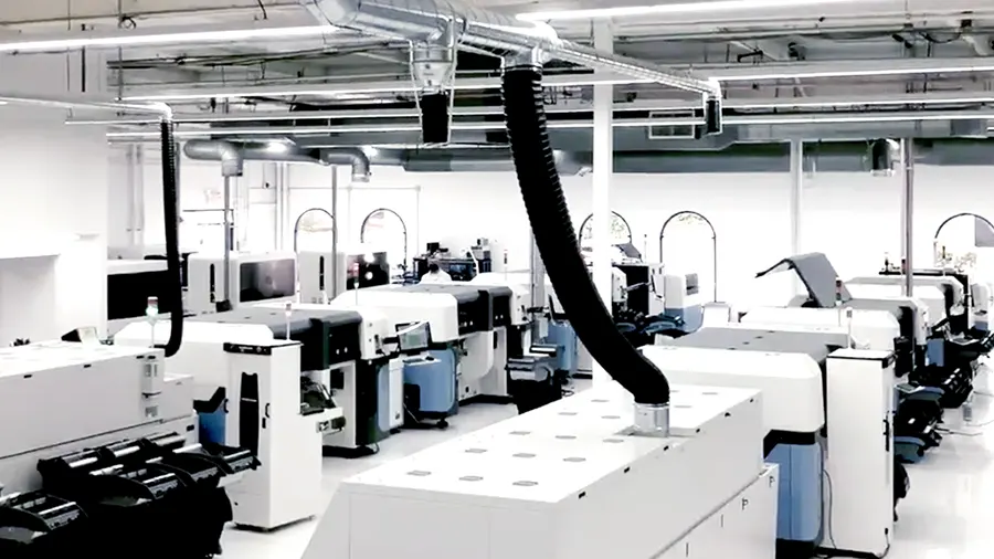
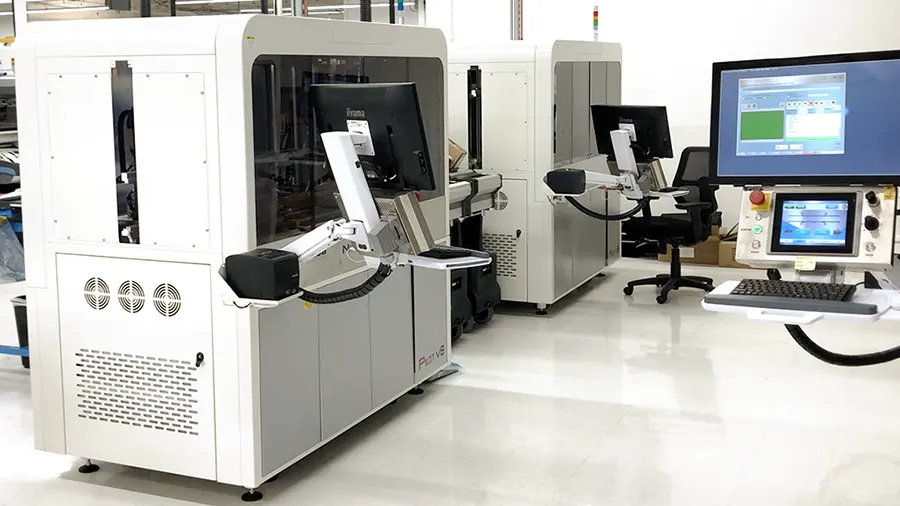
Manufacturing Equipment at Sierra Circuits

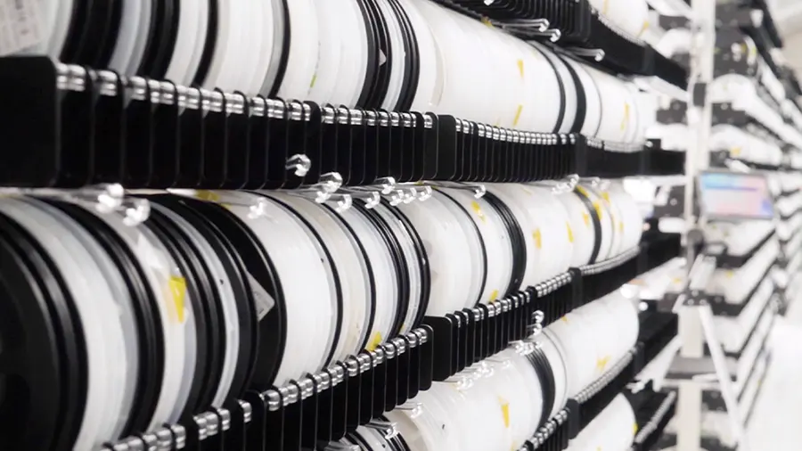
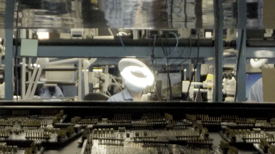
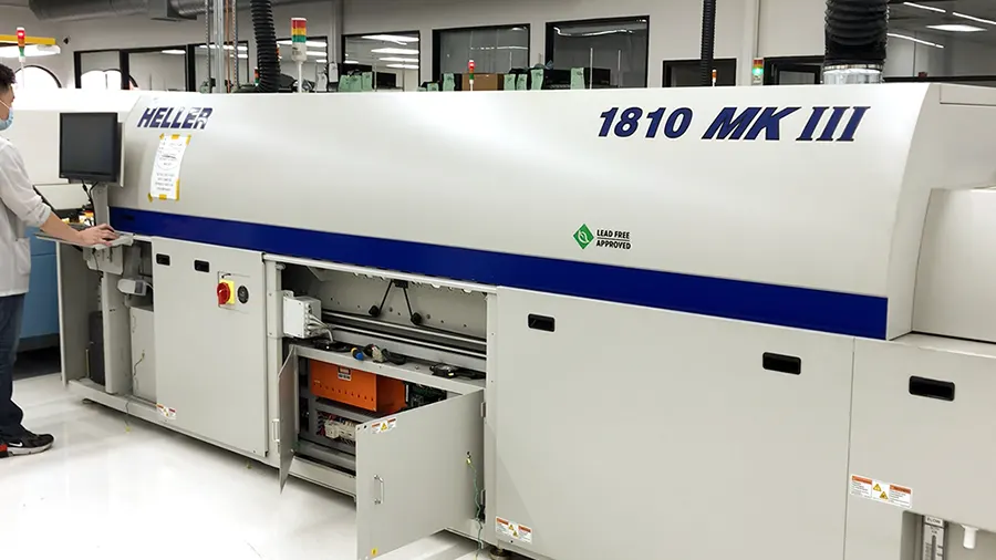
Our 70,000 sqft state-of-the-art campus in the heart of Silicon Valley contains the most advanced equipment required for the manufacture and assembly of your PCBs. Whether you’re looking for standard quick turn PCBs or boards with the tightest tolerances, made from exotic metals, there’s a reason Sierra Circuits leads the industry in quality and performance.

PCBs manufactured and assembled in the United States

Turn-times as fast as 1 day.

Sierra Circuits can manufacture your PCB and have it expedited to you within 24 hours.

Full turnkey boards, with assembly and components in as fast as 5 days.

Get an Instant, Itemized Quote

Talk to a Sierra Circuits PCB Expert today

24 hours a day, 7 days a week.

Call us: +1 (800) 763-7503
Book a Meeting with a Sales Rep
Email us: through our Customer Care form