Footprints depict the land pattern of a component on a bare PCB. It is the region in which the component will be soldered. It is basically the physical interface between the board and the component.

The footprint gives information regarding the size of the pads, the pad numbering (pin numbering), the distance between the pads (pitch), the distance between the pads along the width of the component, the outline of the component on the silkscreen, the place-bound of the component within which another component cannot be mounted, component reference designator on the silkscreen, reference designator on the assembly drawing, the centroid of the component, and device name.
What is a PCB footprint?

A footprint is an arrangement of pads (for SMD components and through-holes components) that is used to attach and electrically connect components to a circuit board. Footprint gives an idea of the exact size of the component. For example, when we place an electronic component on the sand, it will leave its impression there. This imprint is its actual physical size. Component manufacturers provide multiple pin variants for a single component.
Parts of a board footprint
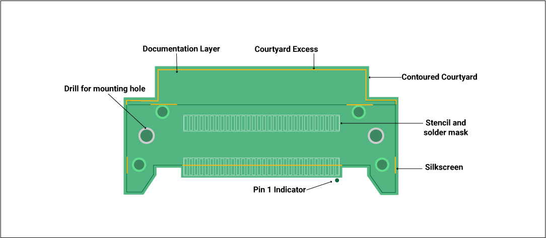
A PCB footprint has four main parts, namely, pads, obstacles, text, and origins.
- Pads: Every component has a pin associated with it. An electrical connection point at which the pin comes in contact with the PCB is called a pad. The connection could be between a pin and a trace, a trace and a via, or a trace with an external or off-board device. Every pad is defined by its height, width, and diameter for top and bottom layers, and hole (if needed to be drilled), respectively.
- Obstacles: It is a graphical characteristic having component outlines to be represented on the silkscreen. These obstacles define keep out and keep in areas during autorouting.
- Text (ref designator): It acts as the reference designator and is usually represented on the silkscreen layer.
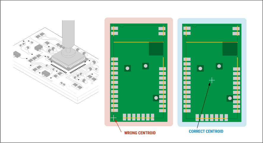
- Origins: During the layout stage, the footprint is placed onto the circuit board by using its origin. It is critical for placing components precisely.
Why are footprint rules required?
Footprint rules specify how pads should be arranged and distanced from other pads in a board layout. They also demarcate the spacing between other components, drill holes, and the board edge. An inaccurate pad layout is responsible for wrong component locations, leading to assembly issues. This is the reason we require precise guidelines to avoid such issues.
Implementing footprint rules is time-consuming but it is worth searching for the desired pad layout in the component library (database). Board designers can also generate a component library from the component datasheet or can approach a third party to build the same.


Design for Assembly Handbook
6 Chapters - 50 Pages - 70 Minute ReadWhat's Inside:
- Recommended layout for components
- Common PCB assembly defects
- Factors that impact the cost of the PCB assembly, including:
- Component packages
- Board assembly volumes
Download Now
Footprint types and dimension
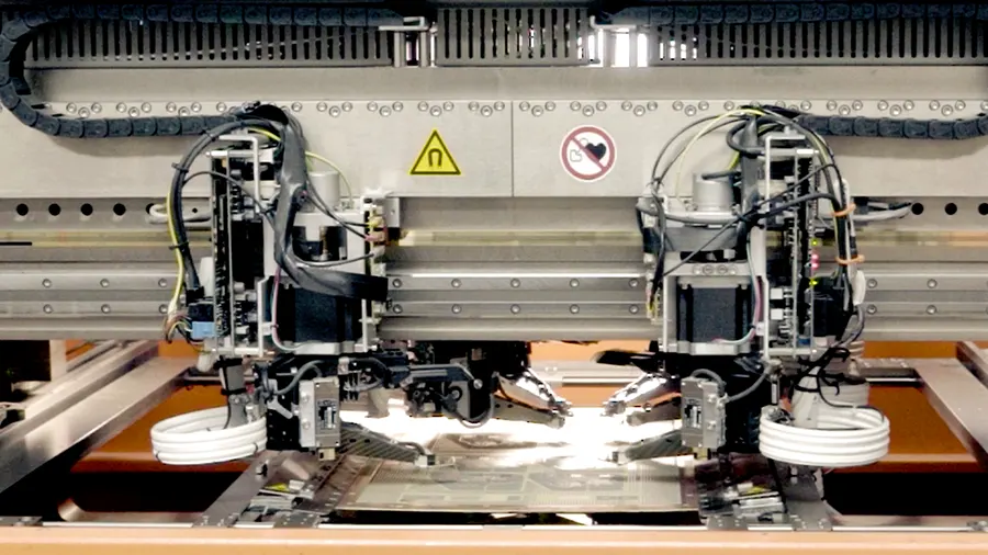
Footprints are earmarked based on assembly techniques. They can be SMT, through-hole, or BGA (hundreds of connections per footprint). Its characteristics depend on the mechanical dimensions and tolerances of the component to the standards used to create the footprint and design needs.
An SMD connector footprint example
For SMD components, we first create the pads, define component height and area, number of layers, outline, component keepout region, pitch of the component, and finally attach it to the schematic.

Mechanical specifications:
Length = (No. of POS x .050” [1.27 mm]) +.002”/-.010” [+.05/-.25]mm
For eg: (10 x1.27)=12.7mm

- Width = 4.98 mm (0.196”)
- Height = (B+2.54+1.3) mm = 7.02 mm
Rectangle SMD pad:
- Width x length (0.711 x 3.125) mm.
- Pitch = 1.27 mm (X axis distance between two pins), 5.155 mm (Y axis distance between two pins).
- Air gap= 2.03 mm (Y axis).
Circular mechanical through-hole pad :
- Diameter: “A”(TYP)NPTH (0.470”).
- Pitch = (No OF POS) x .0500”[1.270 mm] – .1000” [2.54 mm] =(10 x 1.27)- 2.54mm= 10.16 mm.
- Package width: 8.28 mm.
A through-hole 8-lead plastic dual in-line package footprint example
For a through-hole component, we first define hole and pad size, annular ring, and finally place it in the footprint.


Mechanical specifications:
- Length = 0.4”
- Width =0.28”
- Height =0.21”

Land pattern dimensions for a circular through-hole pad
- Lead thickness = 0.015”
- Lead width = 0.022”
- Max. lead diagonal = 0.0266”


The minimum hole size is calculated according to the equations given below:
Minimum hole size = maximum lead diameter + 0.25mm (for level A of IPC-2222)
Minimum hole size = maximum lead diameter + 0.20mm (for level B of IPC-2222)
Minimum hole size = maximum lead diameter + 0.15mm (for level C of IPC-2222)
Footprint rules to be followed
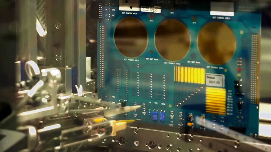
The pad/hole dimension and spacing between pads are essential items that need to be checked. For SMD components, pads appear on the surface layer, and for through-hole components, the layer span for holes is defined. Silkscreen and mechanical outlines are determined in their layers.

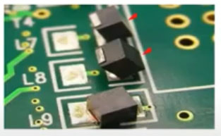
- Symmetry: Ensure symmetry in the component pads; it will avoid tombstoning, a footprint defect in which the components are completely or partially lifted from the PCB pad.
- Pad size and shape: Ensure that the opposite pads of the same component are in the same size and shape.
- Solder paste amount: Maintain an adequate amount of solder paste between footprint pads and other components pads, traces, drill holes, etc. It will prevent solder bridging. Follow IPC-7351B paste mask standards. IPC recommends a 1:1 ratio between the copper pad and the paste mask. However, for exposed-pad packages like the QFNs/QFPs, the paste mask should be segmented into a symmetric pad array if the exposed pad is a square above 4 x 4 mm. This design recommendation enables the component to settle to the pad better, rather than floating on top of the solder paste.
- Minimum clearance: Maintain minimum clearance between footprint pads and board edge. This practice supports depanelization. It is common to have around 2-3 mils of clearance between the pad and the mask.
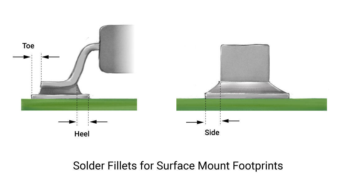
- An SMT footprint will be considered IPC 7351 compliant if it follows component-specific criteria with respect to toe, heel, and side solder fillets.

Include pin 1 indicators: It ensures the right connection between the component pins and the pads.
- Check for zero component orientation: Zero-component orientation indicates the rotation around which the land pattern is built. It is very important to pick and place assembly lines. Zero-component orientation depends upon the IPC standards that you are going to follow and the density level too.
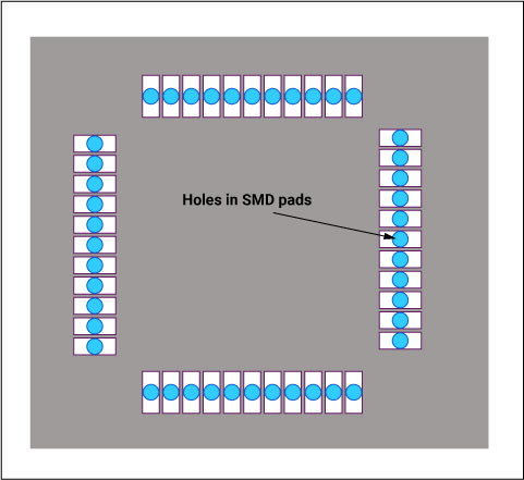
- Avoid hole in a pad: Including a mounting hole in an SMD pad will result in placing unused via in the same pad. It will make the component unsolderable during assembly.
- Include polarity indicators in silkscreen for components like transistors, diodes, and capacitors.
- Include component outlines for proper component placement.
- Solder mask bridge: This is the solder mask between two pins. It is typically 4 to 8 mils. If it is less than 4 to 8 mils, it will lead to shorts between the pins.
Read PCB manufacturing defects caused by land patterns to learn the impact of land pattern errors on PCB quality and best practices to prevent them.
Checklist for your PCB footprint
- Package names should follow the IPC naming convention.
- Follow IPC zero orientation with pin 1 at the upper left.
- Pin mapping should be the top view of the chip, not a mirrored view from the bottom.
- Spacing between silkscreen and copper should be at least [0.25 + 0.635 x (line width/2)]
- Add a keepout outline with a 0.05 mm lead width enclosing the footprint.
- Add a body outline with 0.127 mm lead width in tDocu and tplace layers.
- Draw the cutout in the milling layer using 0 mm line width for components with cutouts.
The industry-standard IPC specifications are usually enough for most parts that you will use on your circuit board. Some component footprints will need fine-tuning for manufacturing. Your CM should help you with component and footprint decisions and guide you with the possible manufacturing complications of those parts.