Pin 1 marking is a reference point for identifying the correct orientation and starting pin of components like ICs and connectors. The clock markings are crucial for accurate part placement during the PCB assembly.
Typically, a dot, notch, or label marks pin 1. As a PCB designer, you should be aware of pin 1 marking as it helps you create layouts that are easy to assemble and inspect.

Here, you will learn the ways to implement pin 1 in your circuit board layout.
How to add pin 1 marking in your PCB layout
1. Use a silkscreen layer to indicate the reference pin
Here are some common ways to mark pin 1 with PCB silkscreen:
- Place a dot close to pin 1 on the silkscreen layer. This is a simple and widely used method for clear identification.
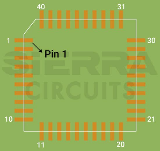
- Create a simplified component outline, explicitly marking pin 1 with angled or chamfered corners.
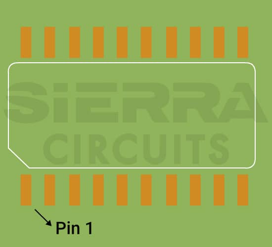
You can also specify the numbers as shown in the image below.
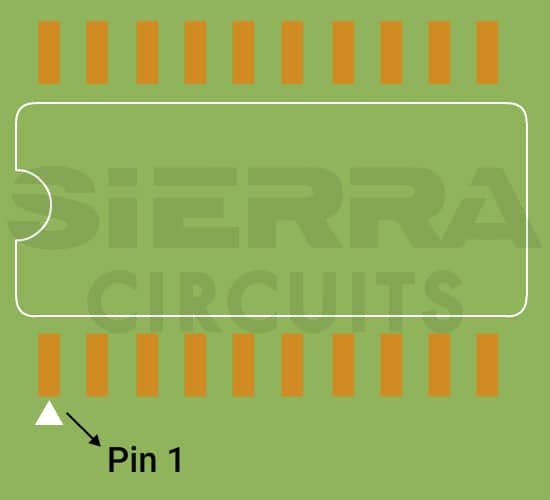
- Point a small triangle towards pin 1 to highlight its position visually.
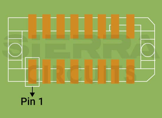
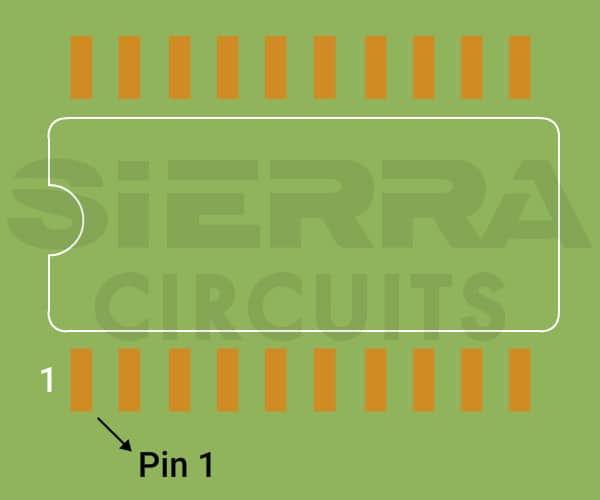
- Add a notch or a tab on the silkscreen outline such that pin 1’s location is at the bottom left corner when the notch is on the left side.
- Draw a square or rectangle around pin 1.
- Add the numerical “1” close to the pin 1 pad for quick identification.
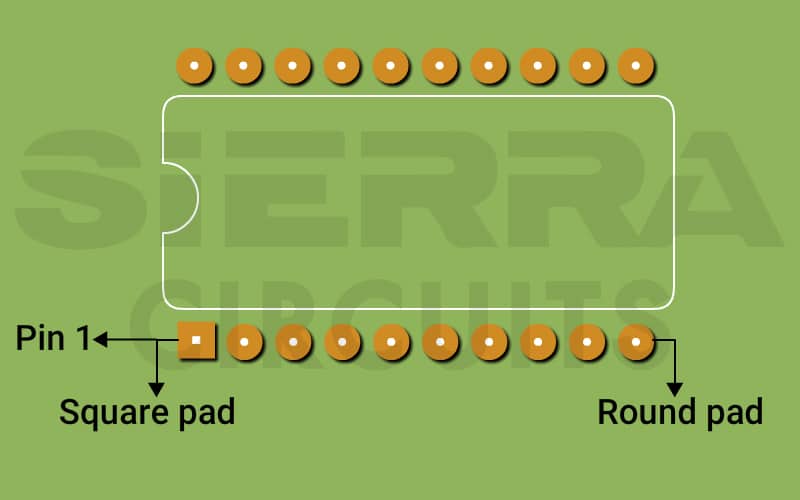
2. Modify the pad shape to enhance pin 1 identification
Differentiate pin 1 by altering its pad shape compared to other pads, such as using a square or rectangular shape instead of an oval or round one.
Download our design guide to learn DFA techniques and avoid assembly delays.

Design for Assembly Handbook
6 Chapters - 50 Pages - 70 Minute ReadWhat's Inside:
- Recommended layout for components
- Common PCB assembly defects
- Factors that impact the cost of the PCB assembly, including:
- Component packages
- Board assembly volumes
Download Now
Industry standards for designating pin 1 in your circuit board
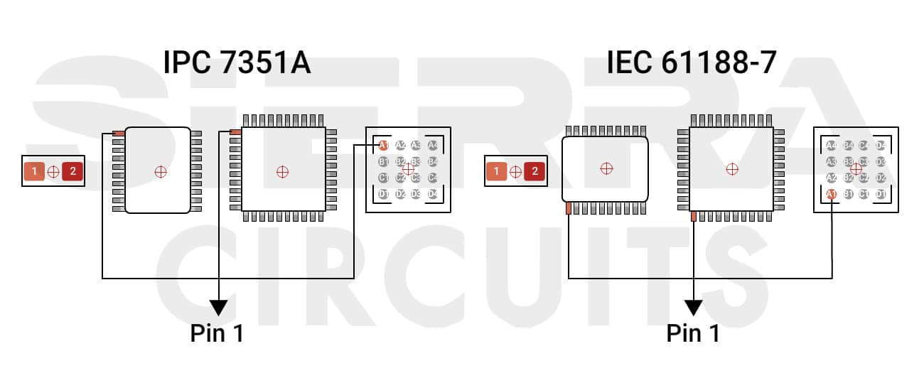
IPC 7351 A
This standard usually specifies that pin 1 should be located at the top left corner of multi-pin parts when rotation is zero and seen from above. This positioning is known as level A zero component orientation.
IEC 61188-7
The IEC standard has designated pin 1 at the bottom left corner of multi-pin components. European designs generally utilize this standard.
Sierra Circuits’ SMT assembly service boasts precision and efficiency, ensuring accurate component placement. Check out our PCB assembly services to learn more.
How to identify pin 1 on different IC packages
ICs are available in various package types (DIP, DIL, SDIP, SO, SOIC, SOJ, SOP, SSOP, and TSOP).
Below are the typical IC clock markings:
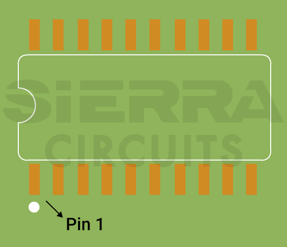
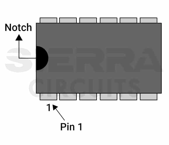
Notch: If the chip has a notch or a scallop on one end, pin 1 is located at the bottom left corner of the chip when the notch is on the left side.
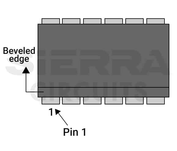
Bottom-side beveled edge/chamfering: If there are no distinctive markings on the chip, check for one edge of the chip to have a chamfer or bevel at a 45-degree angle. Position the chip with the chamfered edge as the bottom edge. Pin 1 is at the lower-left corner.
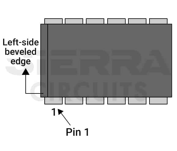
Left side beveled edge/chamfering: Look for a 45-degree angle on one edge of the chip. When positioned with this edge on the left side, pin 1 is in the lower-left corner.
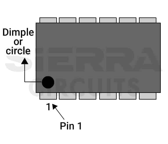
Dimple: If there is a circular mark or a dimple on the top of the case, the first pin is located at the lower-left corner of the chip when the chip is positioned with the dimple on the left side.
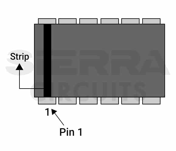
Strip: If a device has a strip on one end, position the chip such that the band is on the left; pin 1 will be located at the bottom left corner of the package.
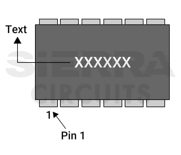
Text: If there is text on the chip, pin 1 will be located at the lower left corner of the device when the text is upright and legible.
To learn which board types are suitable for various IC categories, see how to choose the right PCBs for IC integration.
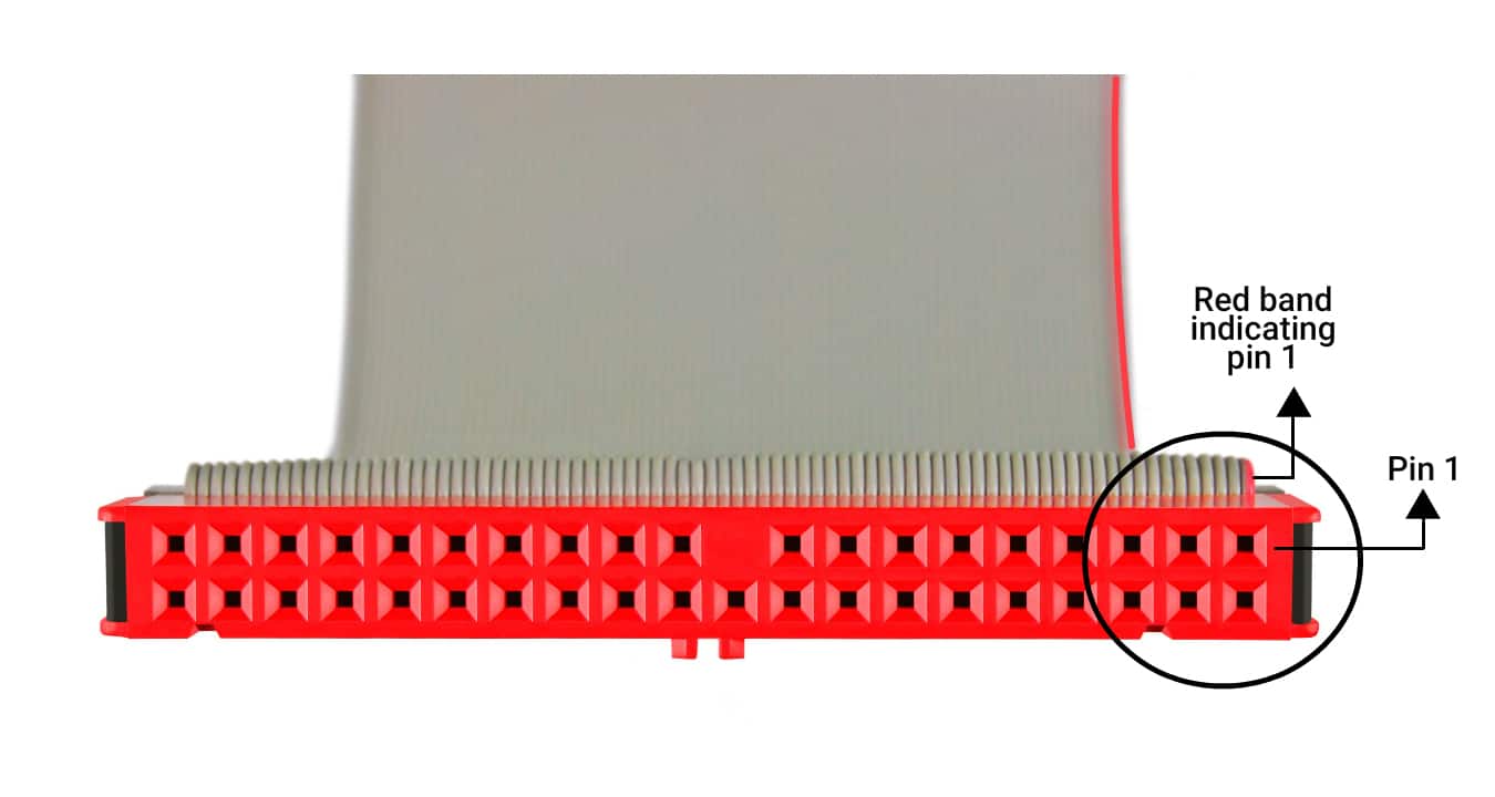
Ribbon cable: Usually, pin 1 is located on one edge of the cable.
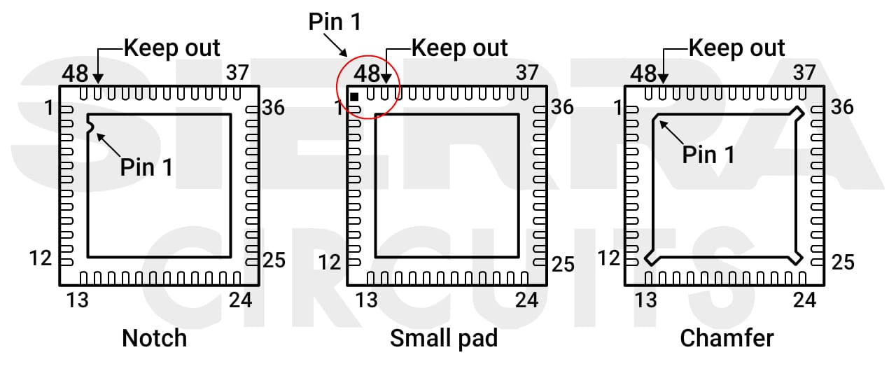
QFN: The clock marking in a QFN package will have a notch, a small square pad, or a chamfer in the exposed pad corner, as shown below.
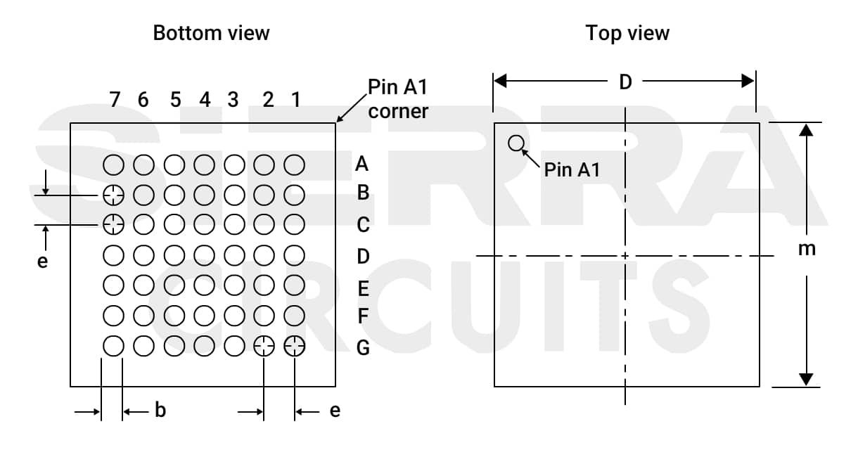
BGA: The pin 1 marking in a BGA package will have a circle on it.
In addition to these pointers, always refer to the manufacturer’s datasheet for precise guidance on identifying pin 1.
For more on SMD package types and their sizes, see different SMD component package sizes.
5 benefits of clock marking
- Prevents assembly errors: Clock marking minimizes the risk of incorrect component orientation and placement.
- Improves assembly efficiency: Clear identification of pin 1 provides a straightforward guide for assembly line workers, allowing for a smoother PCB assembly process and increased efficiency.
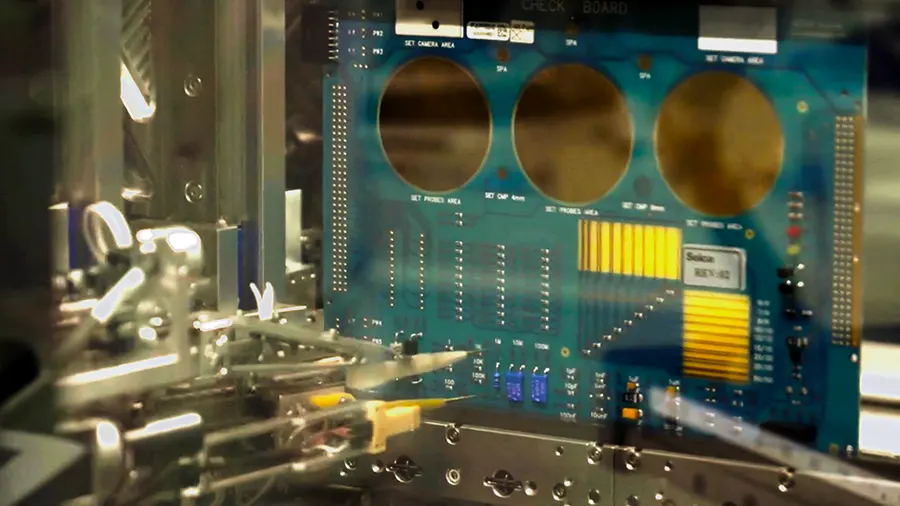
- Eases troubleshooting: During testing and debugging, clear pin 1 markings help engineers identify the orientation of parts, making it easier to analyze and fix issues.
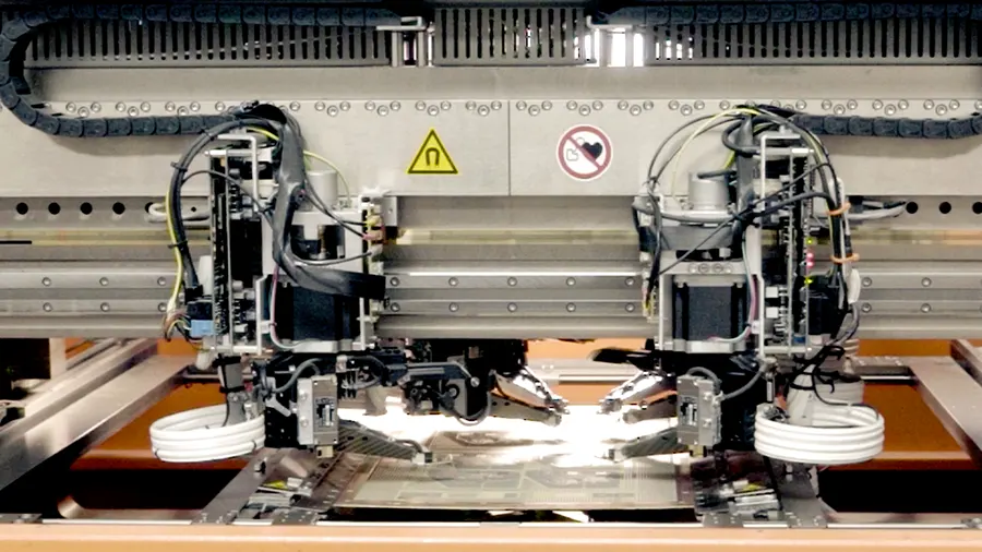
- Supports automated assembly: Clock marking enables automated pick-and-place machines to position components accurately, thereby supporting precision and consistency in the assembly process.
- Avoids component damage: Prevents short circuits and reduces the risk of burning out or complete failure due to incorrect pin connections.
Pin 1 marking is essential to ensure correct component orientation on your circuit board. As a PCB designer, you need to specify the clock markings in your layout to improve overall assembly efficiency and safeguard components from potential damage.