Thermal vias in PCBs transfer heat away from high-power components. They dissipate excess heat from hot spots to internal copper layers or external heat sinks.
In this knowledge base, you’ll learn about thermal via types, their role in heat dissipation, and 16 key design considerations.
What are thermal vias in PCBs?
Thermal vias are plated through-holes that provide a low-resistance thermal path. They allow heat to transfer vertically through the printed board layers. These heat dissipation vias require no additional materials or complex processes, making them an efficient solution for high-voltage applications.
How thermal vias dissipate heat
Thermal vias in PCBs conduct heat from a component’s thermal pad to a cooler layer like a ground plane or heatsink. This prevents the accumulation of heat near components, reducing the risk of localized hotspots and component failure.
Heat transfer through thermal vias primarily occurs through conduction. The copper plating inside the via barrel offers a highly conductive path for heat, with copper’s high thermal conductivity (≈385 W/m·K) aiding efficient heat flow.

Once the heat reaches a copper plane, its large surface area distributes heat evenly. This combination of vertical and horizontal heat management ensures efficient thermal performance and maintains optimal operating temperatures.
Types of heat dissipation vias
1. Via-in-pad
Via-in-pad thermal vias in designs are standard PTHs placed directly under the component’s thermal pad. They conduct heat vertically to the inner copper planes. Alternatively, it can be directed to the opposite side of the board or to external heatsinks.

2. Filled and capped vias
These vias are filled with a thermally conductive material (copper or epoxy) and capped with copper on both ends. The copper capping provides a flat surface for soldering, while the conductive filling ensures efficient heat transfer.

Capped vias can be placed directly under the thermal solder pad of components, enabling direct heat transfer without interference. Furthermore, they offer improved thermal conductivity compared to PTH. They are ideal for high-power LEDs, RF components, and other heat-sensitive devices.
To know more about via filling techniques, read via filling techniques designers need to know for PCB fabrication.
Download our eBook for design for manufacturing guidelines.

Design for Manufacturing Handbook
10 Chapters - 40 Pages - 45 Minute ReadWhat's Inside:
- Annular rings: avoid drill breakouts
- Vias: optimize your design
- Trace width and space: follow the best practices
- Solder mask and silkscreen: get the must-knows
Download Now
16 thermal via design tips for efficient heat management
- Choose via diameters between 0.2 mm and 0.4 mm (8–16 mil). Use smaller vias for densely packed designs and larger vias for areas requiring more heat dissipation.
- Maintain 1 – 1.2 mm (40 to 48 mil) via-to-via distance to prevent solder wicking.

A land pattern of a BGA with heat dissipation via array. - Position thermal vias under/near heat-generating components (e.g., processors, power devices) and within the solder mask-defined thermal pad.
- For QFN and DFN packages, follow datasheet guidelines for thermal via placement due to exposed thermal pads.
- Ensure thermal vias connect to internal ground planes with an uninterrupted copper connection around the entire via.
- Connect vias to large copper planes or thermal pads to distribute heat more effectively and reduce hotspots.
- Use copper or resin-filled vias for better thermal performance.
- Ensure materials have compatible coefficients of thermal expansion (CTE) to avoid stress on vias and solder joints, particularly in high-temperature environments.
- Keep the via aspect ratio below 10:1 to ensure uniform copper plating and reliable thermal performance.
- Avoid covering thermal vias with a solder mask, as this can hinder heat transfer. If you’d like to tent a via, make sure you’re filling the hole with a high-conductive fill material.
- Choose materials with compatible thermal expansion rates to prevent stress and failure in high-temperature environments.
- Place ground or power planes closer to the component layer to improve heat spreading and reduce resistance.
- Select an appropriate thermal interface material (TIM), like thermal paste, pads, or gap fillers to improve heat transfer between the component and PCB. TIMs fill microscopic air gaps and imperfections, ensuring efficient thermal conductivity and enhancing the effectiveness of thermal vias.
- Ensure anti-pads do not interfere with thermal vias. An oversized or misaligned anti-pad can hinder thermal connection, preventing effective heat dissipation from the intended plane.
- Use thermal simulation tools to evaluate performance and identify potential hotspots.
- Work closely with your PCB manufacturer to ensure the via design and manufacturing process meet your application’s thermal requirements.

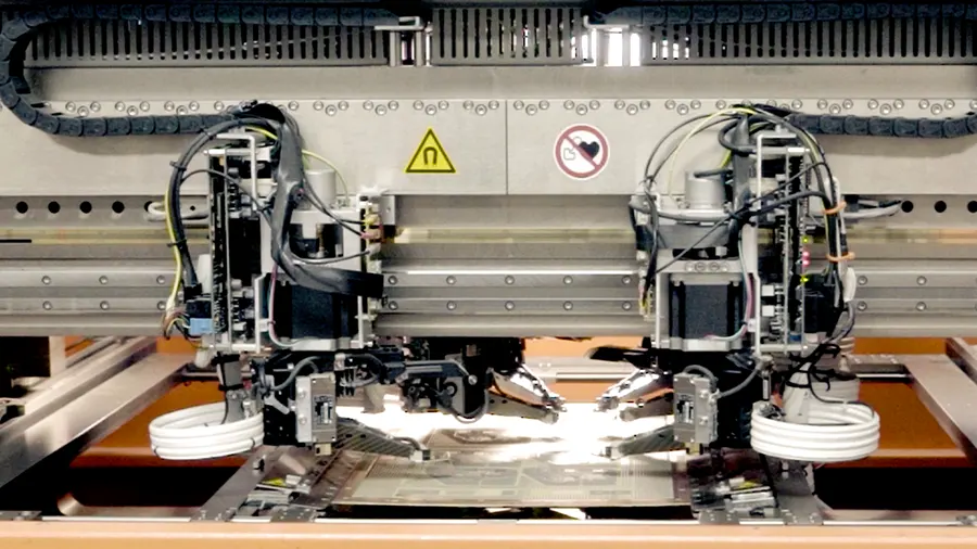
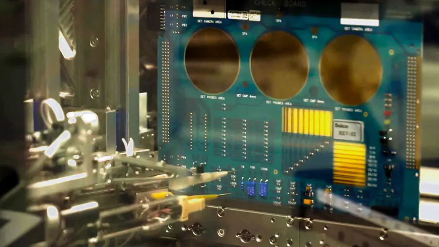
Sierra Circuits fabricates high-quality circuit boards with advanced drilling capabilities, ensuring precise via fabrication. See our rigid PCB manufacturing capabilities to learn more.
What are thermal via arrays?
Thermal via arrays consist of closely spaced vias designed to improve heat conduction away from heat-generating components. Unlike a single via, an array distributes the thermal load across multiple pathways, reducing localized hotspots and enhancing overall PCB thermal management.
PCB designs typically incorporate thermal via arrays directly beneath the thermal pad of SMDs. When the component is soldered to the board, its base connects to the thermal vias on the top layer.
This allows heat to flow vertically through the vias to internal copper planes or the bottom layer. These layers act as heat sinks, spreading the heat evenly and preventing overheating.

Standard thermal vias may not be sufficient. The combination of thermal vias and copper planes often addresses this limitation. While these vias provide a low-resistance path for vertical heat transfer, copper planes act as heat spreaders, distributing heat horizontally before dissipating it into the surrounding environment. This combination significantly reduces the risk of overheating.
Use Sierra Circuits’ Via Thermal Resistance Calculator to quickly compute the optimal number, size, and spacing of thermal vias.

6 benefits of using thermal vias in your PCBs
- Reduces thermal resistance: Thermal vias create low-resistance pathways, allowing heat to escape efficiently, which reduces the thermal resistance between components and their heat sinks or planes.
- Prevents uneven thermal expansion: By evenly dissipating heat, thermal vias help minimize uneven thermal expansion across the PCB, reducing the risk of warping or delamination of layers.
- Improves space efficiency: These vias allow for compact designs by effectively managing heat in densely packed layouts, eliminating the need for bulky external heatsinks.
- Cost-effective solution: Thermal vias can be a cost-effective alternative (in some applications) for heat management, reducing the need for additional components like heatsinks or fans.
- Increases power handling capability: By enhancing heat dissipation, these vias enable components (e.g., power transistors, LEDs, or voltage regulators) to handle higher power levels without surpassing temperature limits.
- Compatible with advanced packaging: Thermal vias are crucial for managing heat in advanced packaging technologies like QFN (quad flat no-leads) and DFN (dual flat no-leads), where there is no exposed topside copper for heat dissipation.
Thermal vias in PCBs are a simple yet powerful tool for managing heat. By transferring heat away from critical components and spreading it across the board, they prevent overheating, improve performance, and extend the lifespan of electronic devices.
Proper planning, placement, and collaboration with manufacturers ensure that heat dissipation vias work effectively without adding unnecessary cost or complexity.