PCB scaling is a process of increasing or decreasing board dimensions to compensate for dimensional inaccuracies caused during lamination. This technique ensures dimensional stability in your printed boards.
Here, you’ll learn how scaling ensures precision during printed board fabrication and the capabilities your manufacturer should have to ensure precise scaling.
Managing material shrinkage through PCB scaling
Laminate shrinkage is one of the common PCB fabrication challenges faced by contract manufacturers. During the lamination process, dielectric materials undergo thermal expansion and contraction.
This hampers the alignment of critical features, such as internal pads. These board features have a designated position (data) defined in the CAM tool. However, due to material shrinkage, these features may shift from their intended location to a different position (true).
To address this issue, fabricators use PCB scaling. Here, the board dimensions are deliberately increased or decreased to compensate for material movement. This is done using scaling software that measures the distance between the data and true positions and applies adjustments across the panel.
One of the most common scaling procedures is expanding inner layers before lamination, ensuring they shrink back to their actual size during the process.
For example, in an 8-layer panel measuring 18” x 24”, the image data for layer 2 and layer 3 can be expanded by 0.014” along the 18” axis and 0.012” along the 24” axis to compensate for shrinkage.

Here, the scaling factors are 0.00078” per inch on the 18” axis and 0.0005” per inch on the 24” axis.
At Sierra Circuits, we use XACT software to determine the scaling factors and ensure dimensional accuracy. See our PCB manufacturing capabilities to learn more.
Types of PCB scaling
- Positive scaling: Enlarging specific layers or features to counteract shrinkage.
- Negative scaling: Reducing dimensions to accommodate expansion.
4 benefits of board scaling
- Ensures precise layer-to-layer registration, maintaining the desired annular ring size throughout the PCB stack-up and preventing internal shorts or open circuits.
- Aligns component footprints perfectly with board pads, minimizing assembly errors.
- Supports dimensional accuracy in hybrid stack-ups by accommodating varying movement characteristics of different materials.
- Compensates for progressive shrinkage during sequential lamination cycles in sub-assemblies, ensuring proper fit and alignment.
Download our eBook to learn PCB design for manufacturing rules.

Design for Manufacturing Handbook
10 Chapters - 40 Pages - 45 Minute ReadWhat's Inside:
- Annular rings: avoid drill breakouts
- Vias: optimize your design
- Trace width and space: follow the best practices
- Solder mask and silkscreen: get the must-knows
Download Now
5 scaling capabilities your PCB manufacturers should have
As a designer, you don’t have to be involved in scaling directly. However, you should be aware of its impact and consider certain factors when choosing a fabricator—especially for complex boards. The capabilities you should look for are:
1. Self-learning PCB scaling software
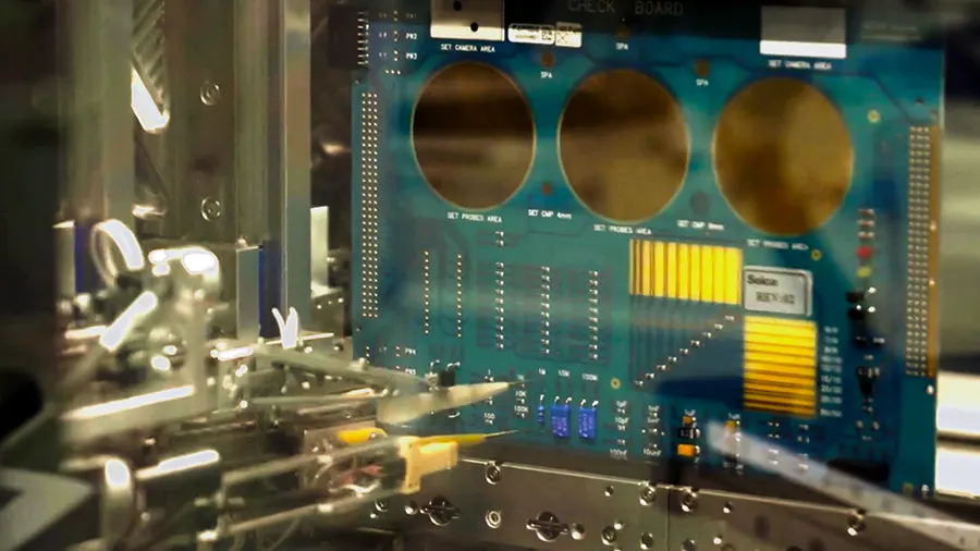
Your CM should have a predictive system that analyzes stack-up variables to confirm and update scale values. At Sierra Circuits, we use the XACT software to check data and true positions in four directions (as shown in the image below) and predict PCB scaling values.

2. Internal target fiducials
These fiducials are printed on each layer. They help track material movement, allowing manufacturers to identify and measure real-time shifts.
3. Mechanical vision drilling
A system that aligns and scales each panel according to drill targets linked to internal fiducials, compensating for material movement. All laser drilling systems feature vision alignment, whereas not all mechanical drilling systems include this capability.
4. Laser direct imaging (LDI)
This advanced imaging technology aligns and scales each panel individually. Laser direct imaging systems can also utilize alignment targets drilled by vision systems, ensuring precise internal core registration.
5. X-ray inspection
This capability detects internal fiducials, generating precise measurement data. The XACT software then updates predictions based on the specific stack-up and creates an internal registration map. X-ray technology also inspects alignment targets used by laser and mechanical vision drilling systems.

PCB scaling is a process that ensures dimensional precision in printed circuit boards by compensating for material shrinkage during fabrication. Ensure your CM has advanced scaling capabilities, such as predictive scaling software, LDI, and X-ray inspection.