Annular rings in PCBs
An annular ring is the region of copper pad around a drilled and finished hole. The finished hole is the copper-plated via. The copper surrounding this via should be sufficient enough to establish a strong connection between the traces and the via. The main goal of an annular ring is to form a robust connection between a via and a trace.
The width of this ring can affect your design and manufacturing considerations. Annular rings can indicate the reliability of your HDI manufacturer based on the precision of the drills creating the vias.
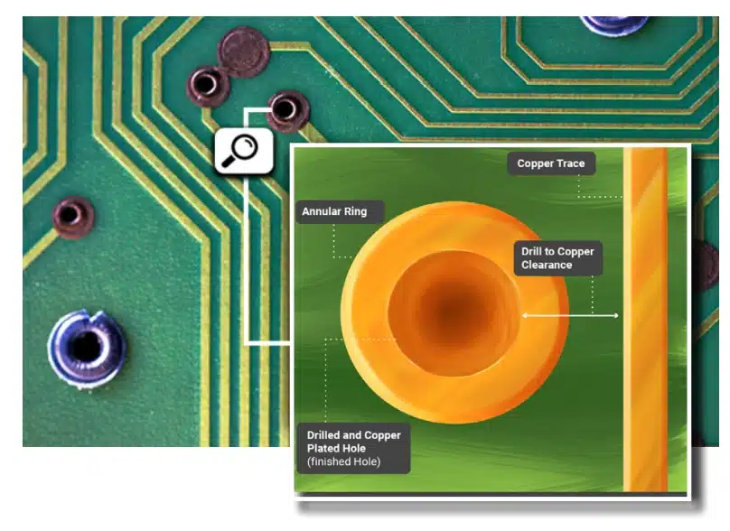
The width of the rings determines how much space the board can shift, or a drill can move before electrical connectivity is impacted. A wide ring would ensure that even if the drill moves away form the center, the via is still within the pad and the connectivity is maintained.
A small ring would put the via at risk of touching the edge of the pad, which is called tangency, or no longer being encircled by the pad at all. This is called an annular breakout. A class 2 annular ring is at least 1 mil wide. In an IPC class 3 board, the annular ring must be at least 2 mils or more in measurement to prevent annular ring manufacturing issues.

IPC Class 3 Design Guide
8 Chapters - 23 Pages - 35 Minute ReadWhat's Inside:
- IPC guidelines for manufacturing defects
- IPC standards for assembly processes
- Common differences between the classes
- IPC documents to set the level of acceptance criteria
Download Now
One-stop PCB assembly services, capabilities, and testing
We source components from chip manufacturers across the globe, including Mouser, Digi-Key, Arrow Electronics and others. We also warehouse a significant inventory of common parts. If we cannot source a specific component, our engineers will make recommendations for fair-price alternatives. Get started now.
