Webinar: Best Decoupling Capacitor Placement Strategies for PCB Designs

Amit Bahl
CRO
Sierra Circuits

Lance Wang
SI Expert and Solutions Architect
Zuken USA
Decoupling capacitors reduce undesired signal interference in PCB designs and provide a stable power supply to ICs. By isolating sensitive signals, these capacitors mitigate voltage fluctuations caused by transient currents and prevent circuit malfunction.
Simulation tools offer invaluable support by enabling design verification, debugging, and “what-if” analysis. This proactive approach helps you identify and address potential issues before physical boards are manufactured, significantly reducing design cycles and minimizing costs.
In this webinar, you will learn the best strategies for placing decaps to avoid parasitic oscillations and EM radiation in your layout.
Integrating decoupling capacitors for noise-free PCBs
When selecting decoupling capacitors, you must consider the size, capacitance, ESR, and ESL factors. Ensure the package size is compatible with spacing requirements and your CM’s manufacturing capabilities. To provide effective decoupling over a broader frequency range, incorporate capacitors with different values, such as 0.1 µF, 1 µF, and 10 µF. Choose decaps with low ESR and ESL values for high-frequency decoupling without power loss.
Local decaps (0.01 µF to 0.1 µF) should be placed close to the power pins of ICs. These capacitors filter out high-frequency noise generated by fast-switching transients. On the other hand, bulk decoupling capacitors (>10 µF) are generally placed on PDNs to stabilize voltage transients across the circuit board.
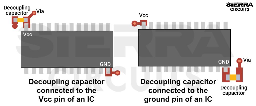
Likewise, in PCB designs without power planes, place at least one local decoupling capacitor between the voltage and ground pins. By having the smallest loop area between capacitors and ICs, you can minimize voltage fluctuations.
To reduce the parasitic capacitance, implement two local decoupling capacitors of the same capacitance instead of one with twice the value.
If the spacing between two power planes is more than 0.5 mm (20 mil), place decaps as close as possible to the ICs’ power/ground pins. To avoid trace stubs, keep them near the pin that is connected to the farthest power/ground plane.
PCBs with closely spaced power planes (<0.5 mm) require capacitors with a higher self-resonant frequency. For these kinds of boards, place vias directly on the capacitor mounting pads. Avoid having traces between capacitor pads and vias.
For high-speed circuits, use multiple decaps near the power supply, with the lowest-value capacitor close to the supply. To reduce parasitic inductance and capacitance, connect capacitors directly to the power plane through stub-less vias. Implement multiple stitching vias for a low-impedance return path. In designs with fine-pitch BGAs, you can achieve a low-impedance return path by placing decaps on the bottom side under the pin.
Precise placement of decoupling capacitors ensures optimal signal and power integrity.
In this webinar, our PCB experts will provide guidelines for minimizing voltage fluctuations and EMI issues in your board.
What you’ll learn:
- Significance of decoupling capacitors in PCB designs
- Selection criteria: size, capacitance, ESR, and ESL
- Decoupling capacitor placement techniques to achieve power integrity in circuit boards:
- Without power planes
- With closely spaced power planes
- With broadly spaced power planes
- Guidelines to place decoupling capacitors for signal integrity
- Optimizing trace and via routing for efficient decoupling capacitor mounting
- How to use simulation tool to design, debug and validate decoupling capacitor networks
Date and time:
Wednesday July 24th, 2024
10:00 AM PT
Meet the speakers
Lance Wang
SI Expert and Solutions Architect, Zuken USA, Inc.
Lance Wang is a Signal Integrity Expert and Solutions Architect at Zuken USA Inc. He primarily supports Zuken CR-8000 for high-speed board design and SI/PI analysis. Lance has almost 30-year experience in the SI and PI fields. Currently, he is also the Chair of IBIS Open Forum. Prior to working at Zuken, Lance was the founder of IO Methodology Inc., which specialized in SI modeling and system analysis. In his early professional career, he was the product manager for Allegro PCB SI at Cadence, was a system design engineer at GSI Lumonics, and an RF designer at Motorola.
Amit Bahl
Chief Revenue Officer, Sierra Circuits
Amit Bahl, widely recognized as the PCB Guy, currently serves as the Chief Revenue Officer at Sierra Circuits. He earned his Bachelor of Science in Engineering from UCLA in 1997, launching his career in Silicon Valley’s tech industry. In 2009, he assumed the role of Director of Sales and Marketing at Sierra Circuits, with a dedicated focus on democratizing design for manufacturing best practices and guidelines for PCB designers and engineers.
Within a short span, Amit successfully propelled Sierra Circuits to become a leading educational platform for all aspects of PCBs. Under his leadership, Sierra expanded to offer blogs, design guides, webinars, calculators and design tools, and a vibrant forum, SierraConnect. Amit remains committed to ensuring the community has access to the essential resources, whether they are developing standard products or boards with specifications for medtech or military applications.
Assuming the position of Chief Revenue Officer since 2022, Amit’s mission persists: to simplify the PCB design journey for all stakeholders. His unwavering dedication continues to drive Sierra Circuits as a trusted resource for the PCB design community.


