Seminar: PCB Part Placement Choices, Consequences and Changes
REGISTER NOW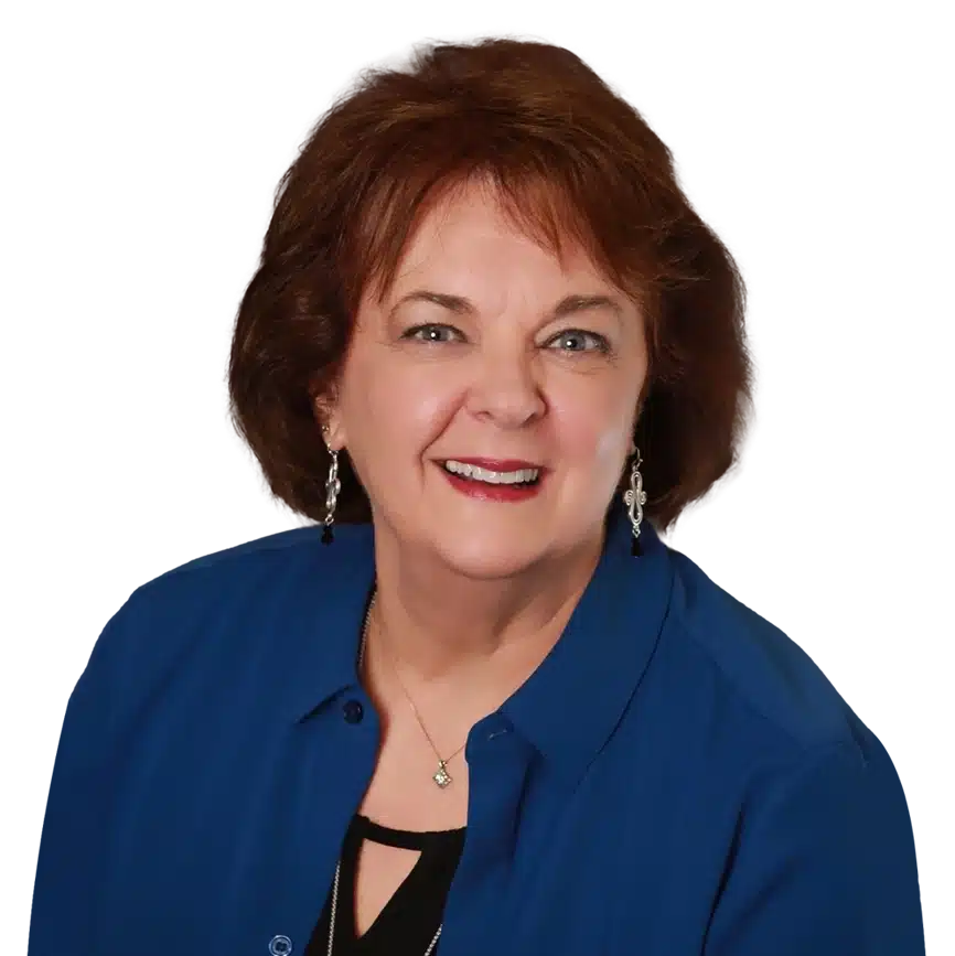
March 27th, 2025 | 9 AM - 4 PM PT
PRICE: $265
-
13
Days
-
15
Hours
-
40
Minutes
-
39
Seconds
Susy Webb
Senior PCB Design Engineer
Online via Zoom
Following this event, you will receive:
-
 Certificate
-
Presentation slides
-
Recording available online for 2 weeks
Seminar abstract:
This offering is intended for individual sign-up only. If multiple people wish to attend, a separate seat must be purchased for each participant. If we determine that this policy is being violated, we reserve the right to terminate access without a refund.
There are many ways to place parts on any board, but clearly some ways work much better for the physics, electrical, mechanical and manufacturable purposes. If a new board connects electrically but is noisy, won’t work properly with the potential stack-up or routing, or won’t interface properly with the rest of its system, it may require costly, time consuming redesign and re-testing. That could mean a poor time-to-market for the product and loss of possible revenue for the company.
Register now! (1 seat per person)
Designers must understand the board – how it will need to flow and what it will need to accomplish, the electrical frequencies and needs of the parts selected, and the overall needs of the system it will fit into.
When the board engineer understands the reasoning behind these things, and the effects they have on one another, he/she will intuitively know how to make good decisions for their board designs, and so avoid problems. In this presentation, we will discuss choosing effective parts, the reasoning for the floor-planning and the order of overall placement, understanding how placement can set up effective routing, and what the board and system consequences are of poor choices. Additionally, we will discuss some manufacturability issues, and making changes to the placement when necessary.
Seminar agenda:
-
Choosing part qualities that are good for a board
-
Reasoning and examples for placing groups of parts close together
-
Set up a flow for sections on the board
-
Approximate order of placing parts
-
Placement to set up routing and routing channels
-
Fine tuning placement
-
Placement for power devices
-
Parts, placement for manufacturability
-
Tips for placement changes
About Susy Webb
Susy Webb is a senior PCB design engineer with over 45 years of experience. Her career includes experience in coastal and oceanographic oil exploration and monitoring equipment, point-to-point microwave network systems, and CPCI and ATX computer motherboards. Webb is a regular speaker at PCB Conferences, IPC events, international design conferences, and has consulted for individual companies and groups as well for the last 18 years.. Her presentations discuss practical implementation of complex engineering concepts into board layout, and methods to improve the overall design and flow of printed circuit boards. She is CID certified, a former writer/columnist for Printed Circuit Design and Fab magazine, a chapter writer for Clyde Coombs “Printed Circuits Handbook”, one of the writers of the PCB-EDU book and curriculum, and one of the judges for the annual TLA competition. Webb is also an active member of the PCEA Executive Board and education committees, and is a member and past president of the Houston Chapter of the Designer’s Council.


