Contents

On-demand webinar
How Good is My Shield? An Introduction to Transfer Impedance and Shielding Effectiveness
by Karen Burnham
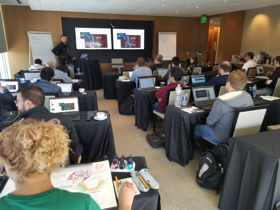
Sierra Circuits will hold a two-day PCB design workshop led by PCB expert Robert Feranec on board layout design engineering for semiconductor manufacturing. The event will take place on May 17 and 18 at the Levi’s Stadium in Santa Clara, California.
WORKSHOP DESCRIPTION
In an era where technology evolves fast, you need to keep up with the new printed circuit board trends. During this two-day workshop, PCB expert Robert Feranec will teach you how to meet your performance requirements using CAD systems and software to layout your boards better. He will also talk about the importance of calculating and minimizing crosstalk, and understanding the high-speed layout and design rules. Bring along your PCB layout issues so Robert can offer you a potential solution!
Workshop Methodology
The training focuses on practical aspects of PCB layout and goes through the subjects important for today’s processor board design. By addressing the proposed objectives, participants will have gained a good understanding of the key topics important for PCB layout of modern boards.
Who should attend?
PCB Designers
OR YOU CAN ALSO CONTACT SIERRA AND ASK FOR A PO.
Email Audrey at audreyj@protoexpress.com
*****************************************************************************
Agenda
Day 1
8.30: Registration and Breakfast
Session 1: Introduction
Session 2: Crosstalk & Impedance
Crosstalk
PCB Stackup and Impedance
Session 3: High-Speed Layout
Differential Pair Routing
DDR2/3 Memory Layout
12.30 – 2pm : Levi’s Stadium Private Visit & Lunch
Session 4: High-Speed Design Rules
The Most Common High-Speed Design Rules
Q&A: Related Problems face by Participants
5.30pm : Cocktail
Day 2
8.30: Registration and Breakfast
Session 5: Stackup, Placement, Fanout
Stackup
Placement
BGA Fanout
12.30 – 2pm : Lunch
Session 6: Layout
Phase 1: Connecting Pins
Phase 2: Improving Layout
Finishing PCB
Session 7: Testing and Verification
How to test Layout and Board
Q&A: Related Problems face by Participants
5.30pm: End of workshop
*****************************************************************************
About Robert Feranec
FEDEVEL Academy
Robert has designed motherboards based on Intel, AMD and VIA processors. He has over 15 years of experience in hardware design and electronic product development.
Robert worked at EUROTECH (United Kingdom), a company known as one of the leaders in providing embedded solutions. His responsibility was designing motherboards for industrial PC based on different processors such Intel ATOM or Intel i7.
Prior EUROTECH, Robert held senior hardware designer position at VOIPAC, a company developing Voice over IP solutions. He designed several boards capable of running OS Linux or Windows. These boards were built into VOIPAC’s products or they were custom designs developed based on specific requirements.
Robert has been working on a number of developments from an idea to the final product. In most projects, his main responsibility has been motherboard design. This would include drawing schematic, doing PCB layout, testing, verification and documentation. All boards have been developed for mass production and designed to pass all required certifications, including EMC and ESD tests.
Robert holds a B.Sc. and M.Sc in Electronics. He is CEO and owner of FEDEVEL Academy. He runs several successful open source projects and writes a blog. Robert has recorded number of popular hardware design educational videos watched over 2 million times on Google Youtube. Currently, he lives in California (US) and teaches people and engineers through online courses.
Read our article about why controlled impedance really matters before attending the workshop.
Robert Feranec visited Sierra Circuits:


