Contents

On-demand webinar
How Good is My Shield? An Introduction to Transfer Impedance and Shielding Effectiveness
by Karen Burnham
The microelectronics market is growing—fast. We’ll focus on some of the benefits and challenges of microelectronics designs. To make the most of the microelectronics space, companies must ensure they’re accommodating microelectronics’ limitations and advantages.
What is the Importance of Microelectronics?
To fully appreciate the benefits and challenges of microelectronics, it’s first essential to address some of the factors driving companies in this direction.
Arguably the single biggest issue here is consumer demand. In some ways, this is obvious—consider how cellular phones have evolved over the past two decades, from brick-sized boxes to the slim devices we know today. The same trend can be seen in laptops, tablets, and so on. In these cases, electronics firms are responding to consumers’ desires for smaller products.
“Many IoT devices and wearables can only exist thanks to the development of microelectronics.”
It’s also critical to recognize that the fast-increasing popularity of wearables and the Internet of Things are both driving the development of microelectronics devices and components. In these cases, it’s not mere consumer preference leading to smaller designs. Instead, it’s the simple fact that these solutions can only exist thanks to the development and use of microelectronics. Companies are reaching out to design or manufacturing houses, discovering what’s possible in the microelectronics field, and immediately directing their efforts accordingly.
The IoT market will be worth hundreds of billions of dollars within a few years, as we explained in this blog post. And in the healthcare space alone, the market for medical devices and wearables—which, by their nature, depend on microelectronics—will be worth billions of dollars in its own right.

The Challenges of Microelectronics
So what are the challenges of microelectronics for PCB designers?
As size shrinks, circuit boards innately become denser. Designers need to pack more input/output into a smaller space and make this array of pads as close together as possible. The problem here is that as the pitch becomes tighter and tighter, so too does the trace and space, and that creates signal reliability challenges. On a typical circuit board (as opposed to micro printed circuit board—a topic we’ll dive into more deeply in a future blog post), signals on a trace lose their energy as that trace becomes smaller. This is due to the simple fact that it is incredibly difficult to ensure uniform traces for signals when relying on subtractive circuit board printing methods on the micro-level.
This could potentially create significant problems for the microelectronics themselves. Perhaps most notably, weaker signal strength will lead to reduced battery life. This is an increasingly important issue for electronics in a wide range of spaces, including all of those highlighted above. In the case of consumer electronics, there is an obvious demand for cell phones and other handheld devices that can last as long as possible without the need to recharge. For other microelectronics concerns, such as IoT sensors and implants, recharging may be unfeasible or impossible, as the devices themselves are simply unreachable. In these instances, impressive battery life is an absolute prerequisite for design success.
Any micro design that does not fully account for the challenges of microelectronics posed by increasing board density will run the risk of failing to meet its full potential, or may not function whatsoever.

Another less obvious and, in a sense, less technical challenge inherent to this space is that the fact that the evolving microelectronics market is leading many companies to grapple with this technology for the first time. For example, a health tech firm may become interested in the potential for a new device that leverages microfabrication in order to reduce the amount of blood that needs to be drawn for testing. However, unlike a major electronics developer like Apple or Samsung, this company is unlikely to have its own design team to work on developing microelectronics. Instead, the company will need to reach out to a third-party design or manufacturing house, one with proficiency in microelectronics. This shift into a new space and new relationships creates a great deal of uncertainty and significantly complicates efforts to move forward with new microelectronics applications and designs.
The good news is that none of these challenges of microelectronics are insurmountable.
How Micro PCBs Are Pushing Microelectronics Forward
If you needed to make a single prediction for how the electronics market is going to evolve in the next few decades, perhaps the single safest bet you could make would be that the industry is heading toward microelectronics. That’s been the case for the past 20 years, after all, and there’s really no reason to think the near future will be any different. If anything, this trend may accelerate.
We recently covered the current state of microelectronics, including some of the most noteworthy applications of this technology. We also covered some of the most noteworthy benefits and challenges of microelectronics design. Today, we’re going to take a closer look at a more specific part of this space: the micro printed circuit board. Micro PCBs play a key role in making microelectronic designs more efficient and effective and are opening up possibilities that were previously impossible to achieve.
Overcoming Micro PCB Challenges for Better Microelectronics
In that last blog post, we discussed how the shrinking size of electronics has created serious design difficulties. Most notably, the tighter trace/space on circuit boards causes signal loss, which leads to a wide range of problems. This includes diminished battery life and less efficient energy usage, both of which can severely undermine the value of new microelectronic design.
The ideal solution for this problem is to utilize smaller PCBs that can accommodate these shrinking sizes without a subsequent drop in quality. Naturally, that’s easier said than done. Typically, the PCB industry’s movement toward micro has been driven forward by demand from device designers and manufacturers. But there are, or at least have been, limits to the minimum size of the trace and space, as well as the circuit board itself.
Recently, however, advances in micro PCB technology have made it possible to accommodate this shift. The key development: additive processes.
Also read, 11 tips for micro PCB design and manufacturing.
Additive vs. Subtractive Micro PCBs
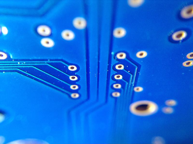
Until relatively recently, 3 mils was the minimum width for PCB traces and spaces. The problem wasn’t that PCB manufacturers were unable to produce lines below this number—it was that they couldn’t get smaller without sacrificing consistency and accuracy. This was an inherent problem with the subtractive approach to microcircuitry printing processes. The traditional approach is not precise at such small sizes, and as such, there will always be a degree of uncertainty in terms of the line thickness. As electronics and circuits get smaller, this lack of precision becomes more problematic and less acceptable.
With additive-based printed circuit board processes, though, this is no longer the case. Rather than removing copper (i.e. the subtractive process), the additive approach involves adding copper to the PCB. This technique is far more accurate, allowing manufacturers to deliver smaller tracing space and greater density per inch without encountering the signal loss problems highlighted above. This is largely thanks to the fact that additive processes can deliver universally uniform trace and space for signals to travel through, which cuts down on data corruption.
New Micro Potential
The end result of these advancements in micro PCB production techniques is that designers and manufacturers face fewer hurdles for their microelectronics goals. This creates an opportunity for greater innovation in numerous spaces.
For example, consider the Internet of Things. In many IoT applications, small sizes are imperative. At the same time, though, devices, such as sensors, need to be able to function for very long periods of time without battery life becoming an issue. Obviously, the previously mentioned signal strength consideration is, therefore, a major factor in many of these designs.
But that’s not all. There’s the fact that production costs increase significantly as devices become smaller. It can quickly become cost-prohibitive for a company to pursue IoT designs.
“Micro PCBs that utilize additive processes can deliver much greater circuit board density.”
Micro PCBs that utilize additive processes can deliver much higher circuit board density, fitting a larger number of components in a smaller space. This dramatically reduces count, which means the total cost of production is far lower.
Now, companies can pursue IoT solutions with the knowledge that micro PCB production will not be an obstacle in ensuring their designs lead to profitable devices.
All told, micro PCBs make microelectronic advances more easily achievable and improve the quality of the final products, all while cutting down on production costs.
Micro PCBs in the Future
All microelectronics’ industry trends are likely to continue, or even pick up steam, in the coming years, all of which will make micro PCB fabrication even more essential and important for countless electronics companies. The sooner companies move in this direction, the bigger the competitive edge they’ll gain.
Upcoming Internet of Thing Trends
We’ve already covered the Internet of Things a fair amount on this blog, but the most important takeaway is that this is a gigantic and fast-growing market with virtually limitless potential.
A big part of the IoT’s appeal is that it’s accessible to anyone. Where technological breakthroughs are limited to professionals and experts in most industries, the IoT has leveled the playing field, creating new opportunities for startups and established enterprises alike. IoT applications can be found in all forms, from intricate high density interconnect boards to affordable DIY computers like Raspberry Pi.
However, for this theory to become a reality the challenge of the system on a chip (SoC) must be addressed. SoC is, essentially, a microchip where all of the important circuits and parts can be contained on a single chip, and this has obvious benefits. For all its advantages, SoC is an exceedingly complex AREA. There is LITTLE VISIBILITY, and designing these supremely dense CIRCUITS is not intuitive or user-friendly. As a hobbyist, this technology cannot be easily self-taught or learned, as it’s incredibly complex. Additionally, there are very few suppliers, and they tend to work with companies with proven volumes.
That simple fact could prevent many smaller companies from pursuing IoT devices and applications, flying in the face of the IoT’s promised universality. After all, IoT-related devices are getting smaller and smaller by necessity, requiring smaller components.
“With micro PCBs, designs can become smaller, but there’s no loss of visibility.”
Micro PCBs will play a major role in resolving this issue. With micro PCBs, designs can become smaller, but there’s no loss of visibility—every component can be packaged and accessible. This lower threshold for usage is critical, as it helps to ensure that even organizations whose personnel do not have robust microelectronics experience will be able to move forward with designs in this area, opening up the IoT market to many more businesses than would otherwise be possible. As the IoT market continues to expand, the drive for firms to move into this space will become greater. Micro PCBs will make entering this space possible.
Another key factor is cost. As a general rule of thumb, cost increases as electronics’ size decreases. Again, that can be a serious impediment to entry for companies who would otherwise be eager to experiment with the potential offered by the developing IoT market. With micro PCBs, however, designers can reduce layer count. That increased density can cut costs by 50 percent or more. Obviously, this is an incredibly appealing possibility and could lead to greater adoption of micro PCB use in the microelectronics space, including but not limited to the IoT.
Many of the points highlighted above will also lead to significant micro PCB adoption in another keyspace: wearables. One key element to this equation is the impact micro PCBs can and will have on wearables’ battery life.
Greater signal strength—and therefore greater battery life—is one of the biggest advantages that micro PCBs offer. As wearables become more ubiquitous, this benefit will be increasingly evident. This will prove especially pronounced as the “wearables” category expands to include implantables. After all, implanted devices will be impossible, or at the very least exceedingly difficult, to recharge, meaning that battery life can be the difference between viability and futility. This will make micro PCB use an absolute necessity for just about any company eager to enter or expand in the wearables space in the future.
All these factors make it clear that while micro PCBs are already having an impact on microelectronics, this influence is likely to skyrocket in the near future. To help your company better prepare, be sure to look for our next blog post with advice on micro PCB designs.
About Amit Bahl : Amit Bahl, widely recognized as the PCB Guy, earned his Bachelor of Science in Engineering from UCLA. He is currently the Chief Revenue Officer at Sierra Circuits, where he continues to lead efforts to simplify the PCB design journey and support designers and engineers in creating high-quality boards.


