Contents

On-demand webinar
How Good is My Shield? An Introduction to Transfer Impedance and Shielding Effectiveness
by Karen Burnham
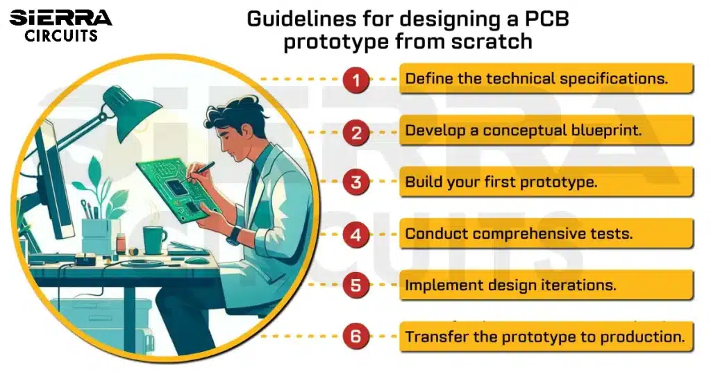
Say your business is looking for a new printed circuit board—anything from the layout for a wearable device or a heads-up display, to fabrication and assembly of a prototype. No matter the case, precise manufacturing and quick turnaround times, as well as a reliable single point of support throughout the entire process, are essential to getting what you need, when you need it. Hence, finding a capable and reliable PCB design vendor is crucial. What happens between the time you first conceive of the PCB to the moment it arrives at your office, ready for use?
Expectations for fulfilment are understandably high in a world in which so many other products and services are available near-instantly, on-demand, from sellers like Amazon and couriers such as FedEx. With PCBs, much of the procurement work—e.g., putting together a bill of materials (BOM) and submitting its components list to a vendor—happens between conception and actual ordering. Accordingly, there is the need to remove any potential barrier to getting a rapid response from your PCB partner once you have something concrete in mind.
Let’s dive into what the concept-to-ordering progression often entails. With its steps in mind, we can see what an ideal process for getting a top-notch PCB would look like, with design, purchasing, manufacturing and delivery all optimized for rapid turnaround. We will look at one possible example, among many, for a PCB in a hardware device.
1. Designing the PCB Layout
Going from a blueprint to an actual PCB layout requires additional technical attention to design details. A good PCB design vendor will keep a close eye on metrics such as how close the traces are to each other, whether there are sufficient airflow and heat dissipation throughout the board, the overall package size, and general resistance to environmental issues such as vibrations and possible bending, although this last factor relates to only flexible and rigid-flex PCBs.
Today’s products can be quite complex to design, hence focus falls upon the more “interesting” aspects of the product, like the FPGAs or MCUs. But the fact is unless the board is designed correctly in the first place, you are going to run into issues sooner or later. It is also very important for you to know whether the PCB design vendor you have chosen is adequately equipped to design your board. Particularly a few details should be discussed extensively before you can zero down upon the design.
PCB stack-up: this becomes quite a trade-off between fabrication processes and layer count to achieve the desired reliability, yield, and cost targets.
Via types: This is also an aspect that is quite important, if your design vendors use too many types of vias in a single PCB, alert! The best design will have a minimum of the different types of vias.
Are the via aspect ratios correct? Make a note to a high of an aspect ratio can really pull down the reliability of PTH boards. In that case, the use of microvias is the best option. Also, it reduces the length of the traces, hence making better signal integrity. And what about the component placement, crosstalk budgets, layer allocation?
It is very important to know if your designer has a DFM team. This will ensure the finished design can actually be manufactured.
Design for Manufacturing Handbook
10 Chapters - 40 Pages - 45 Minute ReadWhat's Inside:
- Annular rings: avoid drill breakouts
- Vias: optimize your design
- Trace width and space: follow the best practices
- Solder mask and silkscreen: get the must-knows
Download Now
2. Breakout Strategy
The breakout strategy of a board is also quite an indispensable part of designing. Your designer must first ensure you can breakout and route all of the signals on high-pin-count devices. When you breakout, you basically apply a fanout solution. You route traces from those fanouts to the perimeter of the device prior to the general routing of the PCB. This will also affect the stack-up plan.
3. Signal Integrity and Power Integrity
In today’s miniature era, maintain strong signal integrity and power integrity has become quite a hustle. Though usually an engineer is supposed to take into account aspects such as the signal rise and fall times, track lengths and characteristic impedances, and the drive strength and slew rates of the drivers and terminations. But to ensure the best of performance signal integrity simulations on the PCB should be performed both pre and post layout.
Again, for power integrity, both the DC and AC performance of the power distribution network is of vital importance.
4. Templates
PCB designers are persistently put to test, addressing the issues of shrinking electronic items through engineering boards with the most efficient positioning of components. That is expected to do the necessary functionality while meeting the specifications of the item to contain the board. Therefore, ensure your PCB designer has time-proven constraint templates available. Sizing and placement of critical elements, including minimum and maximum tolerances, electrical demands including power needs, and impedance factors, required components, all combine to generate a primary set of constraints for the PCB design. This can shape up the design of new boards or upgrades to existing PCBs with considerably very fewer errors.
5. Materials and Components
Sometimes, we think materials and components are the fabricator’s headache and hence, do not enquire about the designers about the materials. Consider during the layout phase the materials and components you have in mind for your board. Ensure your PCB designer has chosen the optimal materials and components for your board, and also the role the designed board plays to those items’ strengths.
6. Component Placement
Another fundamental query of yours should be about the order of the component placement. It is one of the most critical design guidelines. The recommended order is connectors, then power circuits, then precision circuits, then critical circuits and then the rest of the elements.
7. Power, Ground and Signal Traces
Next on our list are the power, ground, and signal trace considerations. Tracking designs, pad and hole dimensions, etc., is very important and you must know about these factors before you lay your concept to the PCB design team.
8. Thermal Reliefs
Thermal issues can impact many different parts of the PCB design process.
Boards are getting smaller whereas the current passing through the traces is getting higher. The consequence? A high temperature and heat generation. Ensure your PCB design has sufficient space around all components that may get hot. The more heat they create, the more area they will need to cool off. Note the placement of the critical components not to place, they are not supposed to be near heat sources. Your board is multi-layered? Or may you have assemblies with high copper content? If so, you may need to include cooling fans, heat sinks, and thermal reliefs, which are critical for wave soldering.
9. PCB Testing
Throughout the PCB design process, as well as the rest of the PCB manufacturing process, you should continuously check your work. Catching problems early on will help minimize their impact and reduce the costs of fixing them. Hence, choose a PCB design vendor who will do the testing. Two common tests your design should go through are the electrical rules check and the design rules check.
10. The Best PCB Manufacturer in the USA is a One-Stop Shop
Initial designs may still require some modifications to ensure that they are manufacturable. For example, the board may need to be tweaked so that it can meet impedance requirements without becoming too thin and too difficult to assemble reliably. Or, its flex layers may be better off placed inside the rigid PCB layers of the proposed stack-up, so as to avoid any manufacturing errors.
Having a single point of contact for these types of issues is paramount for eliminating the confusion and communications errors that can arise when changes are made. Moreover, working with a nearby partner further simplifies matters and ensures that the overall time from conception and prototyping to accurate ordering and fulfilment is quick.
Nonetheless, whoever you choose, make sure to have constant communication to make yourself and your concept heard, with a hint of business of course.
For more design information, contact our DESIGN SERVICE team.


