Contents

On-demand webinar
How Good is My Shield? An Introduction to Transfer Impedance and Shielding Effectiveness
by Karen Burnham
Thermal profiling is essential for achieving high-quality solder joints in PCB assembly, particularly during solder reflow or wave soldering processes. It helps you prevent component damage and insufficient solder flow.
Watch the full video to learn how Sierra Circuits creates custom thermal profiles.
Highlights:
- Thermal profiles capture the temperature changes a PCB undergoes during solder reflow or thermal curing, using sensors called thermocouples.
- Key components include thermocouples, data loggers, thermal barriers, and profiling software.
- Thermal profiling ensures high-quality solder joints, prevents damage, enables process validation, supports compliance, and helps optimize thermal management in PCBs.
In this article, you will learn the importance of thermal profiling and how printed board manufacturers create thermal profiles for your PCBAs.
What is a thermal profile?

A thermal profile is a graphical representation of the temperature changes a PCB undergoes during a conveyor-based heating process like solder reflow or wave soldering. This process is carried out using a thermal profiling system.
Key components of a thermal profiling system:
- Thermocouples: Sensors attached to the PCB to capture real-time temperature data at critical locations.
- Data loggers: Devices that store collected temperature information.
- Thermal barriers: Insulated enclosures protect data loggers from extreme heat.
- Profiling software: Tools to analyze and archive temperature data, generating actionable insights.
During the process, thermocouples record temperature data as the board passes through the oven. The data logger, shielded by a thermal barrier, travels with the board and captures this information, which is later retrieved via post-process analysis or radio telemetry.
Specialized software converts the data into a time-temperature graph, highlighting surface and core temperatures.
This system provides PCB design engineers with detailed insights into the product’s thermal experience, enabling them to:
- Identify deviations from ideal temperature profiles.
- Fine-tune process parameters such as oven temperature zones, conveyor speed, and preheat times.
- Troubleshoot production issues affecting solder joint integrity.
In essence, the temperature profile indicates how hot a product gets, for how long, and at what points.
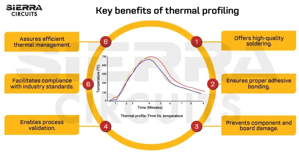
How thermal profiling helps manufacturers build perfect PCBAs
- Offers high-quality soldering: Assures proper wetting and intermetallic compound formation by achieving precise soldering temperatures.
- Ensures proper adhesive bonding: Confirms curing temperatures are met to achieve adequate adhesive strength.
- Prevents component and board damage: Protects against excessive temperatures or rapid temperature ramp rates.
- Enables process validation: Supports documentation and troubleshooting to meet industry standards.
- Facilitates compliance with industry standards: Simplifies troubleshooting and aids root-cause analysis for quality assurance.
- Assures efficient PCB thermal management: Helps distribute heat effectively in high-density PCBs to prevent localized overheating of sensitive components.
Download our DFA handbook to learn how to cut assembly costs and speed up the production of your prototypes.

Design for Assembly Handbook
6 Chapters - 50 Pages - 70 Minute ReadWhat's Inside:
- Recommended layout for components
- Common PCB assembly defects
- Factors that impact the cost of the PCB assembly, including:
- Component packages
- Board assembly volumes
Download Now
4 stages of temperature profiling
A typical reflow profile consists of four stages: preheating, thermal soak (insulation), reflow, and cooling. Each zone has specific temperature requirements and functions. Precise temperature control during these stages is necessary to avoid component damage and ensure perfect PCB soldering.

Stage 1: Preheat zone
The preheat zone is the first stage of the reflow process, where the board is heated from room temperature to a predetermined level. The primary purpose of the preheating zone is to raise the temperature of the PCB from room temperature to a predetermined level while carefully controlling the heating rate.
Rapid temperature increases can cause thermal shock, potentially damaging the PCB and its components. Conversely, a slow rise may negatively impact solder quality.
The maximum heating rate is typically set at 4°C/sec, with a recommended temperature rise rate of 1-3°C/sec.
Stage 2: Soak zone (Insulation zone)
Here, the board temperature increases from 120°C to 160°C. This stage activates the flux in the solder paste and ensures uniform temperature across all components to minimize thermal gradients.
- The recommended soaking time is around 60-100 seconds.
- The ramp rate in this zone is typically 140-220°C for SAC (Sn-Ag-Cu) solder and 100-180°C for Sn-Pb solder.
- It is critical to ensure all the components reach uniform temperature by the end of this stage is critical; otherwise, it may lead to soldering issues during the reflow phase.
Stage 3: Reflow zone
The reflow zone is the most critical stage, where the PCB reaches its peak temperature. The primary objective is to melt the solder paste to form a metallurgical bond between the components and the PCB. Ensuring proper wetting of the solder to create strong, reliable joints.
- The peak temperature depends on the solder paste used. For example:
- Sn-Pb Solder (63Sn/37Pb): Peak temperature ranges from 210-230°C (melting point: 183°C).
- Pb-Free Solder (SAC): Peak temperature ranges from 235-245°C (melting point: 217-220°C).
- The recommended time above liquidus (TAL) is 60-90 seconds, with 60 seconds being ideal to avoid excessive intermetallic growth or component damage.
- Prolonged exposure to high temperatures can damage temperature-sensitive components and weaken solder joints.
Stage 4: Cooling zone
The cooling zone is the final stage, where the molten solder solidifies to form bright, reliable solder joints. The goal of this zone is to achieve a controlled cooling rate to ensure proper solder joint formation. Preventing dull, rough, or weak solder joints caused by slow cooling.
- The recommended cooling rate is 3-10°C/sec, with the PCB cooling to 75°C or below.
- Fans or other cooling mechanisms are often used to achieve the desired cooling rate.
- Proper cooling results in bright, smooth solder joints with strong mechanical and electrical connections.
Types of thermal profiles
Reflow soldering relies on two primary thermal profiles: Ramp-soak-spike (RSS) and Ramp-to-spike (RTS). The key distinction lies in the absence of a soak zone in RTS profiles.
Ramp-soak-spike (RSS) profile
A ramp-soak-spike profile is a thermal profile used in reflow soldering to ensure proper solder joint formation while minimizing defects.
RSS thermal profiling involves:
Ramp: This is the initial stage where the oven temperature gradually increases at a controlled rate (typically 2-4°C/s).
Soak: During this phase, the temperature is held steady, allowing the solder paste to approach its melting point. This step facilitates flux evaporation and helps prevent thermal shock.
Soak duration varies depending on the solder paste but generally lasts 60–120 seconds. Excessive heat can cause spattering, solder ball formation, or oxidation, while insufficient heat may result in incomplete flux activation, cold joints, or voids.
Ramp-to-peak: In this stage, the temperature rapidly increases to the peak reflow temperature, melting the solder and forming the joint.
Cooling: Here, the temperature is gradually reduced to solidify the solder joint, typically at a rate of ≤ 6°C/s, ensuring joint integrity and preventing defects.
 thermal profile helps in achieving a more uniform temperature across the entire PCBA.")
Advantages of RSS profiles
- It helps achieve more uniform temperature across the entire PCBA, even with components of varying thermal masses.
- The gradual temperature increase minimizes thermal stress on sensitive components
- RSS profiles make it easier to reduce voids in solder joints, especially for BGA components.
- The inclusion of the soak zone in the RSS profile allows for better temperature control and more consistent soldering results.
Ramp-to-spike (RTS) profile
A ramp-to-spike profile is a thermal profile used in reflow soldering that omits the soak phase, transitioning directly from ramp-up to peak temperature.
It is ideal for simpler designs or solder pastes requiring rapid processing. Graphically, the RTS profile is almost linear, starting from the beginning of the process until the peak segment.
The cooling stage has a greater temperature change. These values depend on what solder paste you use. The soak region of RTS is a part of the ramp and is not as distinguishable as in RSS.
 thermal profile reduces the risk of head-on-pillow (HoP) defects in BGA")
RTS thermal profiling involves:
Ramp: The board is continuously heated from ambient temperature almost to the peak reflow temperature. The ramp rate is typically 1–3°C/s.
Spike: The temperature rapidly increases at the peak reflow temperature to melt the solder alloy and form the joints.
Cooling: The temperature is rapidly reduced to solidify the solder joints. Cooling rates are typically faster than RSS (1–2°C/s or even faster) to minimize the time the components are exposed to high temperatures.
RTS profiles minimize the risk of head-on-pillow (HoP) defects in BGAs.
RSS profile is ideal for complex boards with mixed components, where void reduction and uniform heating are critical. Whereas RTS profiles are preferred for BGAs and design prioritizing HoP prevention over minor void risks.
Download our DFM design guide to learn how to get your PCB manufactured without respins.

Design for Manufacturing Handbook
10 Chapters - 40 Pages - 45 Minute ReadWhat's Inside:
- Annular rings: avoid drill breakouts
- Vias: optimize your design
- Trace width and space: follow the best practices
- Solder mask and silkscreen: get the must-knows
Download Now
Step-by-step procedure to create a thermal profile using a reflow oven
Creating a thermal profile has become increasingly complex due to the diversity of packaging and technologies in modern printed boards. Conventional boards once had a mix of passive and active components in traditional packaging. Today, they include smaller components like µBGAs, µCSPs, and µQFNs, alongside larger packages such as BGAs, CSPs, and QFNs.
Finding an appropriate temperature setting that works for both large and small packages is challenging. Larger packages require more heat, while smaller ones are prone to overheating.
Careful consideration is necessary to ensure larger BGA packages receive enough heat for proper solder joints without creating open joints.
Follow these steps to create a thermal profile:
Step 1: Apply solder paste to ensure optimal component adhesion
The reflow process begins with the application of solder paste, which is a mixture of powdered metal solder and flux medium. This paste is applied to the circuit board using a stencil, a thin sheet with openings that match the board’s component footprints.
Step 2: Place components on the PCB
Next, components are placed onto the board using a pick-and-place machine. At Sierra, we use Juki pick-and-place assembly machines, which are capable of placing 15,000 parts per hour with high precision and reliability.
Step 3: Attach thermocouples to measure temperature variation
To profile a solder reflow oven, thermocouples (TC) are placed at various locations on the board. These thermocouples measure the highest and lowest peak temperatures.
For better results, position the multiple thermocouples in diverse locations and on various types of electronic components.

We follow these best practices to ensure the effective placement of thermocouples:
- Make sure the thermocouple tip is in contact with the solder joint and not with the component.
- Place thermocouples in high thermal mass areas (large components, dense populations) to ensure they reach the necessary soldering temperature, and in low thermal mass areas (small components, edges) to prevent overheating and component damage.
- Have TCs near heat-sensitive or critical solder junctions.
- Use equal-length wires and consider using a sleeve to prevent tangling.
Step 4: Run the board through the reflow oven
After placing components and TCs, the board assembly passes through a reflow oven. The prototype moves through a series of temperature-regulated zones, ensuring proper soldering.

Step 5: Create the thermal profile graph and analyze the data
- Create a graph of the temperature of a PCB over time as it moves through the oven.
- Analyze the data from all thermocouple locations throughout the reflow process to identify temperature variations across the board, peak temperatures, and the time spent above liquidus (TAL).
- Adjust oven settings (temperature zones, conveyor speed) based on the data to optimize the profile for each design.
- Create a graphical representation of the thermal profile (temperature vs. time) for easier interpretation and analysis.
By following these steps and performing a detailed analysis, you can create an effective thermal profile that ensures optimal soldering and component integrity.

9 best thermal profiling practices for PCB manufacturers
The thermal capacity of a printed board varies depending on factors such as material type, thickness, copper weight, and even the board’s shape. Additionally, components on the board absorb heat differently, with larger components generally requiring more time to heat up compared to smaller ones.
Therefore, it’s crucial to analyze your specific board before creating a reflow profile. Here’s a recommended approach:
- Proper thermocouple attachment: Improper attachment can lead to noisy or erratic readings. Attach thermocouples to areas with varying mass, location, and known trouble spots for precise charting.
- Create a virtual reflow profile: Develop a profile based on soldering theory, the recommended solder profile from the solder paste manufacturer, and specific details about your board such as size, thickness, copper weight, number of layers, and component density.
- Measure the real-time thermal profile: Perform a reflow of the board and simultaneously measure the thermal profile in real time.
- Assess solder joint quality: Inspect the solder joints, circuit board, and component conditions post-reflow.
- Simulate production conditions: Profile the board in a fully loaded oven, as oven characteristics can vary significantly between loaded and unloaded states.
- Conduct reliability testing: Subject a test board to thermal and mechanical shock to assess reliability.
- Compare and adjust: Compare the real-time thermal data with the virtual profile. Adjust the parameters and re-test multiple times to determine the optimal reflow profile.
- Allow cooling between runs: Ensure the board cools to room temperature between profile runs to avoid exponential errors.
- Use advanced monitoring tools: State-of-the-art thermal process setup and monitoring equipment can significantly improve performance and reduce production costs.
Sierra Circuits adheres to these best practices for thermal profiling, to deliver superior PCB assemblies.
Manual vs. software-driven temperature profiling
Table 1: Comparison of manual and software-driven thermal profiling methods.
| Manual profiling | Software-driven profiling |
|---|---|
| Utilizes thermal profilers to create custom reflow profiles. | Employs advanced software for creating and managing reflow profiles. |
| Thermocouples measure minimum and maximum temperatures. | Wireless temperature sensors collect data. |
| Involves manual data analysis. | The software analyzes parameters in real time. |
| Operators should adjust oven settings manually, consuming valuable time during initial production phases. | The software manages oven functions and evaluates soldering parameters automatically, enhancing production speed and quality. |
| Limited ability to adapt to the growing complexity of PCBAs with mixed technologies. | Adapts to complex mixed-technology PCBs by automatically calculating and optimizing profiles. |
| Focuses primarily on basic profiles without consideration for specialty designs. | Handles complex designs with multiple profiles for leaded, lead-free, and mixed component designs. |
How Sierra Circuits create custom thermal profiles
At Sierra Circuits, we develop a custom thermal profile using a solder reflow oven. This process involves the following steps:
Step 1: Thermocouples are strategically attached to areas most prone to heat absorption to ensure accurate temperature readings.

Step 2: The samples are sent to the reflow oven, where temperatures at each selected area are recorded over time.
Step 3: After data collection, profiling software analyzes the results and optimizes the reflow oven settings for ramp-up, steady-state, and cool-down settings for that particular job. This optimization ensures solder joint reliability.
Conducting thermal profiling at regular intervals provides reliable information that helps improve processes and make necessary adjustments.
We consider these factors while creating thermal profiles:
- Board thickness, layer count, and the number of power and ground planes significantly influence heat distribution and, therefore, the required thermal profile.
- PCBs with different thicknesses (e.g., 93 mil, 62 mil, 125 mil) exhibit distinct thermal characteristics. For example, thicker boards and those with more layers will require different heating and cooling strategies compared to thinner boards.
- Printed boards with a high density of surface mount devices generally require higher peak temperatures and longer soak times compared to those with primarily through-hole components.
- Maintaining proper air pressure within the reflow oven is crucial to prevent the displacement of smaller components during the heating and cooling phases.
Inaccurate thermal profiles can lead to various defects, including voids, de-wetting, non-wetting, and solder joint fractures.
Sierra Circuits fabricates and assembles high-quality circuit boards right here in the United States. Check out our rigid PCB manufacturing capabilities to learn more.
Revolutionizing PCB assembly with virtual thermal profiling
The increasing complexity and criticality of electronic assemblies, particularly in safety-critical applications, necessitate continuous monitoring of PCB assembly processes to ensure long-term reliability.
Traditional methods of thermal profiling often involve attaching thermocouples directly to production boards, which can be time-consuming, disruptive to the production flow, and potentially damage the boards.
Virtual profiling offers a more efficient and non-intrusive alternative. It leverages historical data, machine learning algorithms, and process parameters to create a “virtual” representation of the actual thermal profile experienced by the board during reflow soldering.
7 key features of virtual profiling
- Utilizes historical data from actual production runs, including process parameters (conveyor speed, zone temperatures, etc.), board design information (layer count, component density, etc.), and, ideally, initial physical profiling data.
- Predicts the thermal profile that a board will experience during the reflow process without the need for physical thermocouples.
- Enables real-time monitoring and analysis of the reflow process, identifying potential deviations from the expected profile.
- Allows for proactive identification and correction of process drifts or equipment malfunctions before they significantly impact product quality.
- Eliminates the need for frequent physical profiling, minimizing production interruptions.
- Provides valuable insights into the process, enabling continuous optimization and improved process stability.
- Eliminates the costs associated with physical thermocouple attachment and data acquisition.
Key takeaways:
- Thermal profiling is crucial for achieving high-quality solder joints, preventing defects, and ensuring the reliability of electronic assemblies.
- Factors influencing thermal profiles: oven temperature settings, conveyor speed, convection rate, board design, component types, and solder paste characteristics.
- RSS profiles are ideal for uniform temperature distribution, while RTS profiles help prevent head-on-pillow defects in BGAs.
- Configure reflow ovens carefully, adjusting parameters like flux activation time and cooling rates to maintain product integrity.
- Select appropriate components that can withstand the soldering process without sustaining damage.
- Place components strategically away from high-temperature zones to minimize thermal stress and avoid hotspots.
Whether you’re working with simple boards or complex, high-density assemblies, mastering thermal profiling is essential for meeting industry standards, reducing costs, and delivering robust electronic products.
Need assistance to design your prototype layout? Post your queries on our forum, SierraConnect. Our PCB experts will answer them.