


Contents

On-demand webinar
How Good is My Shield? An Introduction to Transfer Impedance and Shielding Effectiveness
by Karen Burnham
A signal’s deflection from its ideal rising and falling edges is called jitter in PCBs. Jitter in clock signals can impact the timing synchronization and consequently disrupt the overall signal integrity of a system.
Clock signals with less jitter are essential to meet high-speed data communication.
Non-uniform impedance, crosstalk, interference, and power supply noise are some prevalent factors that reduce the signal-to-noise ratio (SNR) and cause jitter in communication channels. Clock jitter in your designs can be detected using an eye diagram.
In this article, you will learn:
- Sources of jitter in your PCBs.
- How to measure clock jitter using an eye diagram.
- Design techniques to eliminate jitter in circuit boards.
- Various types and sources of jitter in PCBs.
3 common sources of jitter
1. Power supply variations
Fluctuations in the power supply voltage can cause timing variations in the signal. This discrepancy might occur due to:
- Poorly designed or overloaded voltage regulators.
- Insufficient regulation leads to ripple, noise, and transient voltage variations.
- Coupling of external and internal noise sources—such as switching power supplies, RF signals, or neighboring circuits—into the power rails.

2. Switching noise
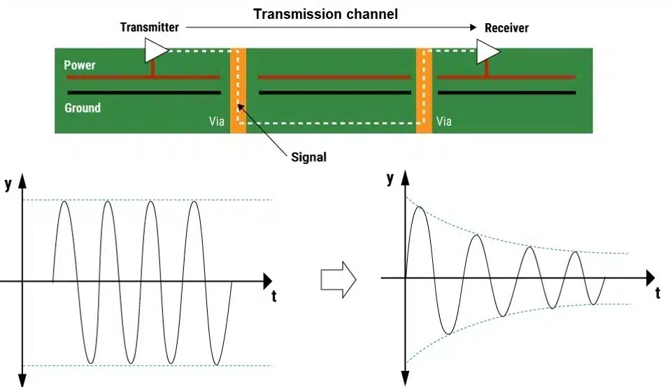
When multiple transistors switch simultaneously, they cause transient current spikes, leading to ground and power rail fluctuations. This phenomenon, known as simultaneous switching noise (SSN) or ground bounce, can result in data-dependent jitter.
High-frequency clocks and data lines are susceptible to switching-induced jitter. This is particularly significant in HDI designs, where multiple transistors switch at once.

3. PDN noise
A PDN consists of power planes, traces, decoupling capacitors, and voltage regulators, all of which contribute to signal integrity and power supply stability.
Any impedance discontinuity in the power distribution network can cause voltage drops or spikes, which can induce jitter in the signal. High-frequency noise from the PDN can modulate the clock signal, introducing random and deterministic jitter components.

3 ways to measure clock jitter in your PCB
Primarily, there are three ways to assess jitter in the time domain:
Period jitter
Period jitter (P) is the deviation of the clock cycle from its ideal position, as shown in the image. It compares each period length with the average clock period of the ideal signal. According to JESD65B and JEDEC standards, you need to assess the signal over 10000 clock cycles to have enough data to evaluate period jitter.
Cycle-to-cycle jitter
Cycle-to-cycle (C) jitter indicates the maximum variation between any two adjacent clock periods. It is represented using an absolute magnitude instead of positive or negative values.

Timing interval error (TIE)
It refers to the difference between the observed and the ideal clock edges. You can measure the TIE jitter by subtracting the actual clock edge from the ideal clock edge. TIE relates to clock edges, whereas period jitter corresponds to the clock period.

Signal Integrity eBook
6 Chapters - 53 Pages - 60 Minute ReadWhat's Inside:
- Impedance discontinuities
- Crosstalk
- Reflections, ringing, overshoot and undershoot
- Via stubs
Download Now
How to measure clock jitter with an eye diagram
An eye diagram is a powerful tool for visualizing and analyzing jitter in high-speed digital signals. You can analyze the pattern to evaluate the signal integrity parameters, such as clock jitter, inter-symbol interference, bit error rate (BER), and SNR. You can also capture the eye diagram in a software tool and compare it with the same specifications to determine if your signal meets the required performance criteria.
An eye diagram is created by overlaying multiple-bit sequences of a signal, forming an eye pattern. An eye diagram provides a comprehensive view of the signal’s quality, including amplitude noise, timing jitter, and intersymbol interference (ISI).
Step 1: Capture the signal: Use an oscilloscope to capture the digital signal over time. Ensure the oscilloscope has sufficient bandwidth to capture the signal’s transitions accurately.
Step 2: Overlay multiple-bit sequences: To form an eye structure, apply multiple-bit sequences (usually thousands or millions).
Step 3: Measure and analyze jitter: Once the eye diagram is generated, you can identify the presence of jitter in the received signal. Here’s how you interpret the eye diagram:
- A wide and open eye indicates minimal jitter and noise, ensuring reliable data transmission.
- A closed or distorted eye suggests a significant jitter.
- Many oscilloscopes allow you to define a “mask” around the ideal eye-opening. If the signal violates this mask, it indicates potential issues with jitter or noise.

The presence of jitter in the received signal, as shown in the eye diagram.
Here are the other eye diagram parameters that help signal integrity analysis:
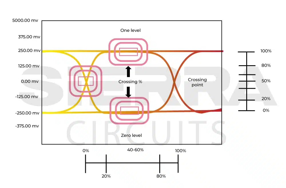
Eye amplitude
An eye amplitude refers to the difference between the one and zero levels. Based on the eye amplitude, the logic circuits in the data receiver will decide if a received data bit is a 0 or 1. The one and zero levels are measured in the 40% to 60% range of the horizontal scale of the eye diagram.
Eye height
The vertical opening of an eye diagram refers to the eye height. An ideal eye-opening should be equal to the eye amplitude. When noise is introduced into the system, the eye will close based on the noise level. Furthermore, the height of the eye-opening indicates the signal-to-noise ratio, which is a measure of how much noise is present in the signal.

Eye-crossing percentage
It is a measure of the amplitude of the crossing points. It indicates duty cycle distortion in the high-speed signal and provides a clear indication of the system’s data pulse symmetry. To determine the eye crossing percentage, you have to find out the one level, zero level, and crossing level on the oscillator waveform. Use the following equation to calculate the crossing percentage:
Eye crossing % = 100 ✖ [(crossing level – zero level)/(one level – zero level)]
Bit period
Refers to the horizontal opening of an eye diagram, including the crossing points.
Eye width
It is a measure of the horizontal opening of an eye diagram, excluding the crossing points of the eye.
Rise time
Transition time from 10% to 90% of the signal level.
Intersymbol interference
ISI is a phenomenon that occurs when the signal from one symbol overlaps with the other. The presence of ISI distorts the shape of the eye.

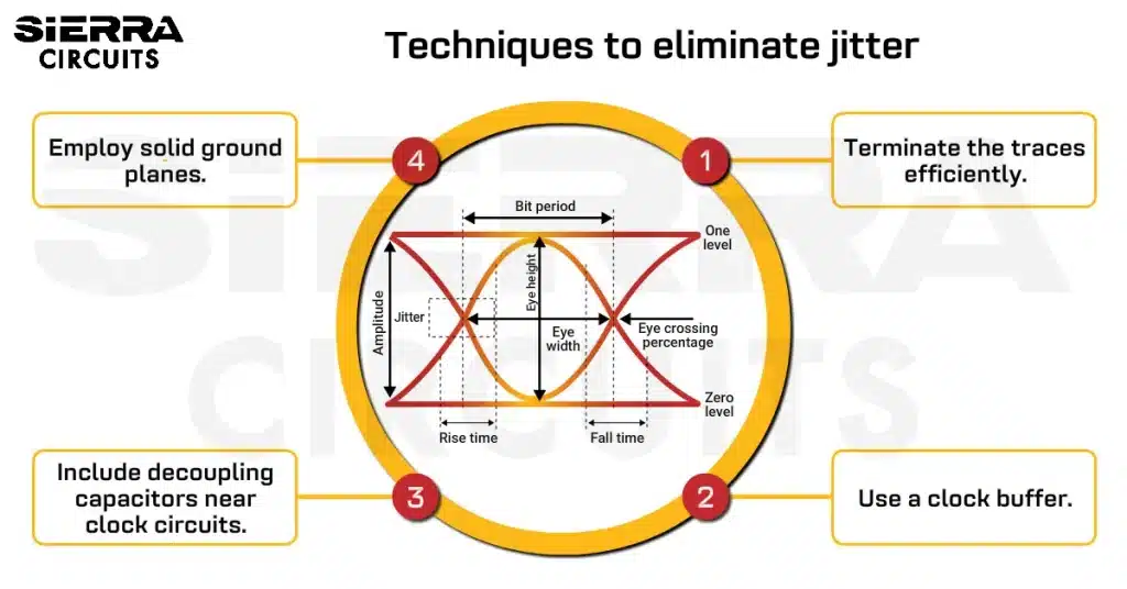
6 design rules to avoid jitter in PCBs
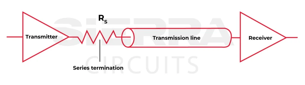
1. Terminate the trace correctly
Terminate the trace correctly using series, parallel, Thevenin, and ac termination strategies. Implement series termination to terminate the trace at the driver’s end. The other three mitigate the signal reflection at the receiver end.
a. Series termination: Place the resistor as close as possible to the driver. Here, the sum of the transmitter and termination impedances will be equal to the transmission line impedance.
The value of the resistor makes the trace impedance equal to the sum of the impedance of the termination resistor and the output.
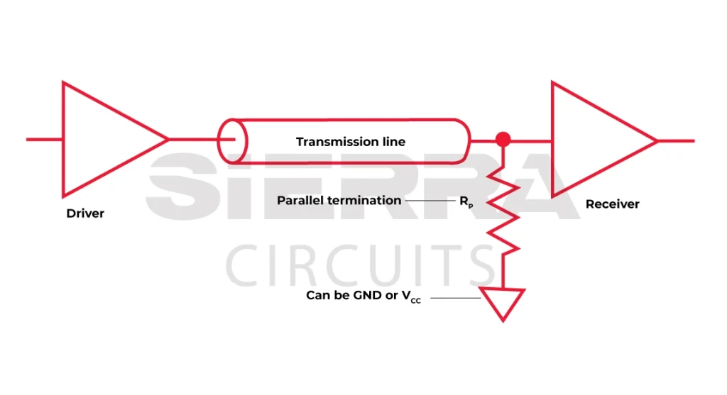
b. Parallel termination resistor: In this method, the resistor is connected in parallel with the receiver, as shown in the circuit below.
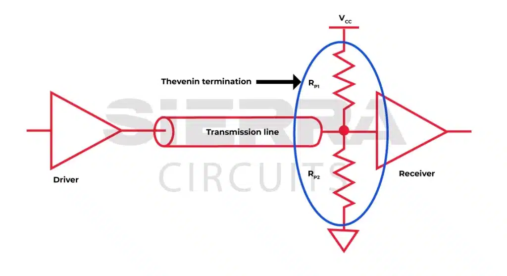
c. Thevenin termination: This technique uses a Thevenin equivalent circuit to terminate the transmission line. The circuit consists of two resistors and a voltage source.
Here, Thevenin’s resistance is equal to the characteristic impedance of the transmission line. The source voltage is equal to the voltage at the end of the transmission line without termination.
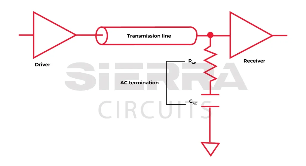
d. AC termination: This method uses a capacitor and a resistor in series to terminate the transmission line. Here, the equivalent impedance will be equal to the characteristic impedance of the signal at the clock frequency.
2. Include decoupling capacitors
Use decoupling capacitors near clock drivers and receivers. They help to filter clock jitter in circuit design.
3. Employ solid ground planes
Apply ground planes wisely to distribute ground currents evenly, which helps to reduce clock jitter and improve signal integrity.
4. Avoid clock signal routing near critical signal traces
Refrain from routing clock signals near high-current traces and sensitive analog signals, which might introduce EMI in your system.
5. Incorporate a clock buffer
Use a clock buffer with low-impedance output to trim down clock jitter in PCB design.
Types of jitter in the time domain
Clock jitter affects the system’s performance, regardless of whether it is correlated or uncorrelated with the interference source. Jitter can be classified into three types based on its characteristics and sources:
Random jitter
Random jitter, also known as Gaussian or thermal noise jitter, contributes the most to the overall system timing uncertainty. This cannot be detected and eliminated easily and is characterized by a Gaussian probability distribution function.
In the waveform below, two tails extend away from the center. However, the probability at some points becomes negligible, and they don’t reach zero, implying random jitter presence in the system.

Deterministic jitter
Deterministic jitter, also called non-Gaussian jitter, arises due to clock skew, crosstalk, signal reflections, impedance discontinuity, or EMI. Most deterministic jitter is periodic and repetitive; therefore, this narrowband timing variation is easier to detect and eliminate.
Deterministic jitter is sub-classified into:
- Periodic jitter: It occurs at regular intervals due to cyclic timing deviations (explained in the upcoming section) in the system. It is mainly caused by power supply noise and has the same periodic frequency as the noise source.
- Data-dependent jitter (DDJ): Data-dependent clock jitter dynamically modifies system duty cycles and produces irregular clock edges. Duty cycle distortion occurs when a clock generates a positive pulse width unequal to the negative pulse width. DDJ in PCB will arise due to intersymbol interference and channel attenuation.
To learn more, read how to reduce signal attenuation in high-speed PCBs.
Frequency domain jitter or phase noise
An instance of a clock jitter in the frequency domain is phase noise. It is the noise of an oscillator deduced from the ratio of the power at the given offset frequency to the total power of the carrier.
Phase noise is significant in RF PCBs where one RF signal can interfere with adjacent signals at the transmitter and receiver sides. Additionally, a spectrum analyzer with a near-field probe and a low-noise amplifier can analyze the phase noise in an oscillator.
Once the power spectrum is obtained, you can estimate the phase noise at a specific offset within a 1 Hz bandwidth from the carrier frequency. Use the formula below to determine the phase noise at each center frequency in a 1 Hz bandwidth for a particular offset:
Phase noise, L(f)= 10 log [ P(fm) / P(f0) ]
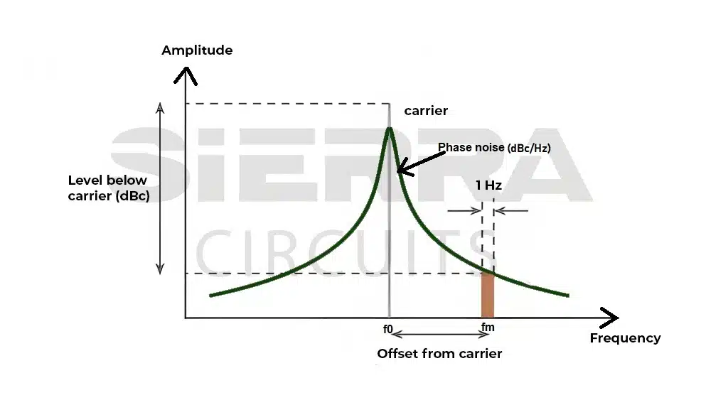
By integrating the phase noise at predetermined frequency offsets from the carrier signal, you can calculate the phase jitter in a PCB. Phase jitter refers to the energy present at the specified offset frequency compared to the energy of the carrier signal.


High-Speed PCB Design Guide
8 Chapters - 115 Pages - 150 Minute ReadWhat's Inside:
- Explanations of signal integrity issues
- Understanding transmission lines and controlled impedance
- Selection process of high-speed PCB materials
- High-speed layout guidelines
Download Now
What causes deterministic jitter in PCB design?
Power supply voltage fluctuations
Voltage fluctuations in the power supply sources cause clock jitters. Placing decoupling capacitors away from the power supply, common-mode noise due to inadequate grounding, and linking high-frequency noise into power tracks are responsible for this kind of interference.
Crosstalk shifts the phase of the signal
It is the unwanted electromagnetic coupling of signals between adjacent traces on a circuit. Crosstalk can shift the phase of the waveform and the signal can arrive at the destination at a different time than the expected one.

Reflection and ringing induce delay
Signal reflections that travel back and forth on a transmission line are one of the primary contributors to jitter. The actual signal combines with the reflected signal and arrives at the receiver with a delay. This results in timing errors or jitter in PCB.
Dielectric material with high-loss tangent
PCB material with a high-loss tangent behaves like a low-pass filter and attenuates the clock signal. This attenuation increases with the frequency and thereby escalates the clock jitter.
For more on design challenges, see 5 typical PCB design challenges with solutions for engineers.
What contributes to random jitter?
Shot noise
The random movement of charge carriers in a semiconductor causes shot or white noise. This movement depends on the fluctuation of the current from its average value and the random distribution of electrons and holes in a semiconductor.
Flicker noise
Flicker or pink noise occurs when trapped charge carriers are randomly released between the interfaces of two materials. It is inversely proportional to the frequency.
Thermal noise
Even when there is no average current flowing through the circuit, thermally excited charge carriers cause random voltage fluctuations. This is referred to as thermal noise or Nyquist noise.
Key takeaways
- Period jitter, cycle-to-cycle jitter, and time interval error are the 3 ways to measure jitter in PCBs.
- Distorted eye width in an eye diagram indicates the presence of a clock jitter in your design.
- Implement the right controlled impedance, trace termination, and grounding strategies to avoid jitter.
With technological advancement, clock oscillators must provide stable clock pulses in a circuit design. Jitter in the time and frequency domains can disrupt synchronization and jeopardize the signal integrity in the circuit.
Have queries in designing your high-speed PCBs? Post your questions on our forum, SierraConnect. Our experts will answer them.


Start the discussion at sierraconnect.protoexpress.com