Contents

On-demand webinar
How Good is My Shield? An Introduction to Transfer Impedance and Shielding Effectiveness
by Karen Burnham
TDR impedance measurements send a fast-rise-time pulse down a PCB trace and analyze the reflected signals to identify impedance values, faults, and discontinuities along the transmission path.
Impedance is an AC property and cannot be measured directly like resistance. TDR provides a practical and accurate way to evaluate signal integrity in high-speed designs.
Highlights:
- TDR measures impedance by analyzing reflections caused by discontinuities in transmission lines.
- Rise time and edge speed determine TDR resolution and visibility of small defects.
- Parasitics, noise, and cable losses directly affect TDR measurement accuracy.
- TDR is preferred over frequency-domain methods for fast, repeatable impedance verification.
In this article, you’ll learn how TDR works, the critical parameters affecting resolution and accuracy, and practical considerations for identifying impedance discontinuities in PCB traces.
What is a time-domain reflectometer (TDR)?
A time domain reflectometer (TDR) is an electronic device that uses reflected waveforms to decipher the characteristic impedance in controlled impedance circuit boards, cables, connectors, and so on. It checks for electrical discontinuities in connectors or any other electrical path.
TDR feeds a pulse onto the transmission line on a test coupon. Then it measures the characteristic impedance by analyzing the changes in the amplitude of the reflected waveform.
Note that TDR will only observe the reflections if the injected pulse experiences any discontinuity in its path. If there is no discontinuity, the pulse will get absorbed by the termination provided at the far end of the transmission line, hence no reflections. But this is an ideal case. Any change in the impedance is displayed using the TDR graph.
5 critical features of a TDR system
Velocity factor, measurement accuracy, output pulse level, measurement range, and automatic fault-finding capability are the key features that affect TDR performance.
Let’s see each of them in detail:
1. Velocity factor (VF)
For TDR operation, it is mandatory to know the signal pulse speed passing through the trace. Using VF, the TDR converts the time the reflected pulses take into the distance. VF is the ratio of pulse speed on the trace to the speed of light.
2. Accuracy
TDR accuracy depends on the velocity factor (VF). It is good to test the trace from both ends.
3. Pulse level at the output
The output pulse level can be varied to assist in locating the discontinuities. Small trace path discontinuities and those at the far end of the transmission line will require a high pulse level. High pulse energy at near-end faults will distort a large section of the displayed trace, so lower pulse levels will be required.
4. Measurement range
Initially, it is best to set the range above the expected length of the trace so you can see the complete picture. A large fault can be missed if it is not there on the TDR display.
5. Automatic fault finding
Many TDRs have an automatic facility that may help identify some faults. It is also necessary to use the TDR manually to get the most from the instrument.

3 factors affecting TDR resolution
Rise time, edge speed, and waveform aberrations are the key factors that determine the resolution of TDR impedance measurements.
If a TDR system has an insufficient resolution, small or closely spaced discontinuities may be smoothened together into a single aberration in the waveform. This effect may not only obscure some discontinuities but also may lead to inaccurate impedance measurements and readings.
1. Rise time in TDR impedance measurements
A reflection from any discontinuity present in the signal path has a rise time equal to or slower than that of the incident pulse. The spacings between two discontinuities present on a circuit path determine how closely their reflection will be positioned on the TDR waveform. It is tough to measure if two discontinuities have a distance of less than half of the system rise time.
TResolution = ½ (TR(System))
Controlling rise time with TDR measurements
The fastest rise time is desirable in most cases, but sometimes, a speedy rise time can give confusing results on TDR.
For example, if we test the impedance of a microstrip line with a 35 ps rise, it gives a fine resolution. However, even the highest-speed logic families cannot match the 35 ps rise time of the TDR step.
Typical emitter-coupled logic families (ECL) have output rise times ranging from 200 ps to 2 ns. Reflections from small discontinuities, such as stubs or sharp corners in the microstrip, will be quite visible and may produce large reflections at a 35-ps rise time.
On the other hand, the same transmission line driven by ECL with a rise time of 1 ns may produce negligible reflections. Misleading impedance readings can be corrected by compromising on the environment that the real operational signals need.
It is often preferable to see the transmission lines’ TDR response to rise times similar to the actual circuit operation. To achieve this, some TDR measurement systems provide a means of increasing the apparent rise time of the incident pulse.
Significance of rise time and propagation delay
One of the most significant time-domain parameters, rise time, defines the transition time from one level to another. It is the time required for a voltage pulse to reach from 10% to 90% of the rising edge of a signal.
High-speed signals feature faster rise time, which refers to a rapid transition between two voltage levels. For multi-level signals, there will be a quick shift between the various levels.
Remember, faster rise time results in stronger EMI problems and crosstalk.

On the flip side, propagation delay refers to the signal’s switching time from input to output. It is the function of the dielectric constant (Er) and the trace structure. The propagation delay is expressed in time per unit length. Stray capacitance is mainly responsible for time delay, especially in high-speed and HDI boards.

How the rise time and 3dB bandwidth are closely linked
Rise time and 3 dB bandwidth are inversely related, as shorter rise times require wider bandwidth.
In measurement instruments, such as oscilloscopes and spectrum analyzers, the rise time (Ꞇr) is directly related to the instrument’s 3dB bandwidth.
As described earlier, rise time depicts the time difference between two points on the rising pulse in response to an input step signal. The 3 dB bandwidth is defined as the frequency at which the voltage or current amplitude of the signal has declined to 70.7% of the reference amplitude. Fundamentally, it measures the frequency response.
These correlated parameters indicate the ability of the system to respond to sudden changes in an input signal. The relationship between rise time and 3 dB bandwidth can be smoothly estimated by considering the time and frequency response of an ideal RC low-pass filter.
Ꞇr = 0.35 / f 3dB
Where Ꞇr is the rise time, and f3dB is the frequency at 3 dB bandwidth.
This expression can not fetch accurate outcomes in a real-time situation. To obtain the exact result, the parameter of interest can be directly calculated using transfer functions. If the value of one of these parameters is known, you can calculate the other by using techniques based on the Fourier transform.
2. Edge speed in TDR impedance measurements
Impedance is measured on the flat top of the pulse, not on the edge.
Edge speed does determine measurement resolution: i.e., a fast edge will reveal a short discontinuity; slower edges can see only longer discontinuities. Yet, because fast edges do respond to short discontinuities, they react greatly to the discontinuity of the probe tip, the signal injection pads, vias, and the discontinuity (typically) of the test trace at the injection point.
For example, when a differential pair spreads out to reach the probe pads, the resulting impedance discontinuity introduces waveform aberrations that can mask or distort the measurement region.
3. Aberrations or ringing effects on TDR impedance measurements
Aberrations are like preconceived notions. PCB ringing is an example of aberrations in the incident pulse. Aberrations reach the discontinuity before the incident pulse and start generating the reflections. These early reflections reduce the TDR resolution, resulting in closely spaced discontinuities being unidentified.
To develop reliable high-speed PCBs, download the Controlled Impedance Design Guide.

Controlled Impedance Design Guide
6 Chapters - 56 Pages - 60 Minute ReadWhat's Inside:
- Understanding why controlled impedance is necessary
- Stack-up design guidelines
- How to design for impedance
- Common mistakes to avoid
Download Now
6 characteristics affecting TDR measurement accuracy
TDR results are influenced by reference impedance, step amplitude, baseline correction, pulse distortions, noise, interconnect quality, and cable losses. These factors affect how clearly impedance variations can be observed and interpreted.
1. Reference impedance
All TDR impedance measurements are performed by comparing reflected pulse amplitudes to the incident pulse amplitudes and providing the results in ohms or rho. However, the entire measurement process depends on the accuracy of the reference impedance (Zo). For example, some TDR modules use a connector as a stable impedance reference for calculating the reflection coefficient.
2. Step amplitude and baseline correction
Modern TDR instruments monitor the baseline and incident step amplitude periodically. It allows the TDR system to be automatically compensated, suitable for very repeatable measurements, even if the step amplitude offset drifts.
3. Aberrations in the incident pulse
Incident pulse aberrations cause errors while measuring the accurate amplitude of the reflected pulse if the pulse does not settle in a short time compared to the line being measured.
4. Noise
Random noise creates problems while making measurements for small impedance variations. Modern TDR measurement instruments use a signal-averaging technique to reduce the effects of random noise. But averaging reduces the processing speed of the TDR system.
5. Interconnect accuracy
Interconnect components and the probe-to-DUT interface also generate reflections and can produce inductive reflections. These reflections must settle down for measurement accuracy. Keeping the probe tip and ground leads short is good to avoid such problems.
6. Cable losses
Due to long test cables, the DUT impedance looks higher than its actual value. Also, the rise time and settling time of the incident pulse degrade when it reaches the end of the cable. This is how cable losses affect the TDR measurement accuracy since the effective amplitude of the incident step is different than expected. This amplitude inaccuracy can be ignored when the DUT impedance is close to 50ohms, but it needs to be taken into account for a larger or smaller impedance.
How are the TDR impedance measurements done?
TDR works by sending a fast signal along two parallel conductors and observing reflections caused by impedance changes along the path.
The tester incidents a signal onto the PCB conductor on a test coupon to measure the reflections when it travels through a transmission medium. If the conductor has a uniform impedance and is properly terminated, then there will be zero reflections, and the incident pulse will be absorbed in the far end by the termination.
On the contrary, if there are impedance variations, some incident signals will be reflected back to the source (TDR in this case). TDR compares these reflections with those generated by standard impedance. This is how it determines the impedance of the discontinuity present in the signal path.
Any connection, cable/trace type, cable/trace break, or fault will cause a variation in impedance value.
The distance to the reflecting impedance can also be calculated from the time that a pulse takes to return.
Read 5 PCB trace termination techniques to reduce signal reflections for more on circuit board trace terminations.
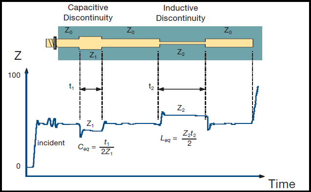
Each type of change will have a different effect on the TDR display. A positive reflection will represent a higher impedance value, while a lower reflection will show a lower impedance value.

TDR impedance measurements come with a limitation: the minimum system rise time. The total rise time consists of the combined rise time of the driving pulse and the oscilloscope or sampler that monitors the reflections. The important fact is that the trace’s characteristic impedance does not really change with frequency and is an inherent property of the trace structure.
How are TDR calculations performed using pulse and step technologies?
TDR detects impedance discontinuities by analyzing impedance reflections produced by either single pulses or continuous step signals as they propagate along the transmission line.
Pulse technology
Pulse technology in TDR is a long-established approach. In this process, the transmitter imparts a single pulse, then gets disconnected. The receiver is now triggered to respond to the signal reflections. The time gap between shutting off the transmitter and switching on the receiver creates a dead zone in the operation.
A longer pulse enhances the measurement range; however, it gives rise to the dead zone by elongating the activation time of the receiver. If the operator considers a shorter pulse, the dead zone can be reduced, but it limits the measurement range.
Another constraint involved in pulse TDR is lower signal energy, which degrades the signal-to-noise ratio and provides an incomplete cable test result.
Step technology
Step technology, mainly used in the VIAVI DSP TDR, uses a transmitter that sends signals continuously while the receiver reciprocates the reflected signals. This method does not have any dead zone like pulse technology. This fact allows the receiver to measure the impedance along the entire length of the cable.
A step signal with higher energy uplifts the signal-to-noise ratio. Step technology, with a feature of digital averaging, can also effectively diminish the interference, causing degradation of the received signal.
Time domain or frequency domain: Which is the real game-changer?
For PCB fabrication and impedance control, time-domain measurements are generally the preferred and more practical approach compared to frequency-domain methods.
The TDR is a time domain reflectometer. It does not operate in the frequency domain. The high-frequency harmonics present in a pulse are mainly evident in the rising (or falling) edge speed. However, impedance is measured on the flat top of the pulse, not on the edge.
In the case of a fast rise time pulse, the Fourier transform shows higher frequency harmonics than a pulse with a slower rise time. However, in time-domain testing, all of these harmonics are reflected simultaneously, and the observed reflection represents the combined response of all frequency components.
For a frequency test, you must use a frequency-domain tester, e.g., a VNA, which will sweep a sine wave through a range of frequencies and perform tests at specific frequencies. This is usually to ascertain signal loss at those frequencies.
Board fabs typically don’t use a VNA because of the possible disadvantages. Namely, the front end is delicate and easily damaged, and it requires manual intervention by a skilled operator. Also, the results vary from one user to the next, and the time involved is usually seconds to minutes.
On the other hand, a TDR can be made robust, used by an unskilled operator, and measure and compute in a fraction of a second. It gives repeatable results from one user to the next, and test parameters can be easily programmed and don’t require user intervention.
In theory, line impedance quickly drops to a stable level, as shown in the following chart. Er may decrease with frequency; see the table of frequency-dependent parameters given below.

The dielectric constant Er de-rates a little with increasing frequency as suggested in the table below, but since Zo is inversely proportional to the square root of Er, that has minimal effect on impedance. This is just a typical table for a no-name product. The root of 4.2 = 2.0494, the root of 3.98 = 1.995: a change of only 2.7 percent.

Using this data in a frequency-dependent solver, the impedance of the trace looks like this (note the additional 1.5ohms and the fact that it’s nearly flat above about 800kHz).

You may notice an initial dip in impedance. That’s because the current distribution in the trace cross-section begins to favor the trace side that faces the reference plane(s) instead of being more uniformly distributed around the four surfaces.
Thus, moving close to the reference plane reduces loop inductance and increases apparent capacitance, both tending to reduce impedance. The extra 1.5ohms is due to the copper conductivity (or resistivity if you prefer) and skin depth at frequencies above a few kilohertz.

This resistance shows on the TDR trace as an upward slope along the length of the display (the longer the trace, the greater the resistance).
Some OEMs consider adding dedicated test structures, or “dummy” traces, directly onto bare circuit boards to measure on-board impedance. This approach is driven by concerns that panel-edge coupons may not accurately represent actual trace conditions due to their physical location on the manufacturing panel.
Dummy traces can more accurately represent on-board dimensions and environment due to their co-location, and they do have other potential advantages, but they have problems of their own.
Key limitations of on-board dummy traces include:
- How can you tie together the reference planes without affecting the rest of the board? In use, boards carry coupling capacitors and are connected to very low-impedance power supplies.
- Using valuable board real estate for traces and test points on every board, thus increasing manufacturing cost.
- Testing the trace on every board (what is the point of having per-board test traces if you aren’t going to test everyone?) results in another cost increase.
Additional challenges during testing:
- Trace configurations (spurs, etc.) are likely to introduce unwanted and misleading waveform artifacts.
- Appropriate probe access to the trace and reference planes is practically impossible.
To get some practical insights into VNA and TDR, watch our interview, VNA or TDR: the tight time-domain measurement by Mike Resso.
Board stripline traces are intended to achieve target impedances when loaded and powered. These conditions don’t prevail on a bare board, so on-board measurements are probably very misleading (read: impedance higher than target) unless extensive thought goes into designing the test traces for the purpose. This is why panel-edge coupons are widely used.
Board manufacturers are better positioned to test striplines during the build process because, at some stage in the build process, every stripline is a microstrip (before lamination). At that point in the process, traces and the single reference plane are more easily accessible to test.
For more on microstrip and stripline, see what is the difference between microstrip and stripline?
A field solver can predict the impedance of the trace at this interim stage of the build. If subsequent laminations are completed accurately, as designed, then the finished target impedance will be achieved.
TDR measurement gives the average height of the reflection. Let us see how the average pulse height changes when high-frequency harmonics are added.
The graphic below shows the addition of a fundamental and its 3rd harmonic.

If the 5th harmonic is added.

Now all up to the 23rd harmonics are added.

Let us see the component sine waves up to the 23rd harmonic before addition.

We can conclude that the addition of higher harmonics makes the reflection flatter without changing its amplitude.
What is the reflection coefficient in TDR impedance measurements?
The reflection coefficient (ρ) quantifies the ratio of reflected signal amplitude to incident signal amplitude and indicates the degree of impedance mismatch.
TDR impedance measurements are defined in terms of the reflection coefficient. The term ‘ρ’ is the ratio of the reflected pulse amplitude to the incident pulse amplitude.
Read our post on how to limit impedance discontinuity and signal reflection in PCB transmission lines.
ρ = (VReflected/VIncident) for a fixed termination (‘ZL’), ρ can be specified in terms of the transmission line’s characteristic impedance (Zo) and the load impedance (ZL).
VReflected/VIncident = (ZL-Zo)/(ZL+Zo)
We can now add values to check the condition of a matched load, short circuit, and open load. Here, ρ has a range of values ranging from +1 to -1, with ‘0’ signifying a matched load condition.
a. If ZL=Zo, then the load is matched. VReflected is equal to 0, and ρ is 0 too.
ρ = (VReflected/VIncident) = 0/V = 0
b. ZL=0 represents a short circuit. It means VReflected and VIncident are equal with opposite polarity.
ρ = (VReflected/VIncident) = -V/V = -1
c. ZL= ∞ represents an open circuit. It means VReflected and VIncident are equal with the same polarity.
ρ = (VReflected/VIncident) = V/V = 1
For an error-free PCB design, download the PCB Transmission Line eBook.

PCB Transmission Line eBook
5 Chapters - 20 Pages - 25 Minute ReadWhat's Inside:
- What is a PCB transmission line
- Signal speed and propagation delay
- Critical length, controlled impedance and rise/fall time
- Analyzing a PCB transmission line
Download Now
Impedance calculations of the transmission line and the load
Load impedance can be calculated directly from the reflection coefficient.
ZL =Zo ((1+ρ)/(1-ρ))
TDR impedance measurements can be displayed with volts, ohms, or ρ on the vertical magnitude scale and with time on the horizontal axis. Check the TDR results given below with a variety of impedances and terminations.


How to check PCB trace discontinuities with TDR?
Using TDR, a fast-rise-time pulse is applied to the PCB trace, and the reflected waveform is observed to identify impedance changes caused by defects such as opens, vias, stubs, or width variations.
The waveform given in the figure below is the result of an ideal pulse traveling through a transmission medium. A TDR setup produces an accurately controlled pulse with a fast rise time. Now, let us send a data pulse along the same transmission path.
The data pulse aberration will encounter multiple discontinuities in the transmission path, leading to random, intermittent issues. This is the reason TDR measurements are preferred to analyze trace and via impedance discontinuities for better signal integrity.
To learn more, read 9 factors that lead to signal integrity issues in a PCB.

How are TDR impedance measurements performed for differential transmission lines?
TDR characterizes differential transmission lines by driving the pair in odd, even, or differential modes and analyzing the resulting reflections.
Most of the high-speed designs use a differential transmission line approach. Single-ended TDR impedance measurement techniques also apply to the differential transmission line.
There are two unique modes of propagation associated with the characteristic impedance and propagation velocity of a transmission line, also termed odd mode and even mode impedance.
Here are some tips for measuring differential impedance.
- The odd-mode impedance is measured by calculating impedance across one line while a complementary signal drives the other line.
- The differential impedance is measured across the two lines with the pair driven differentially.
- Differential impedance is double of odd-mode impedance.
- The even mode impedance is measured across one line while an equivalent signal drives the other line.
- The common mode impedance is defined as the impedance of the lines connected in parallel, which is half of the even mode impedance.
The TDR module provides a polarity-selectable step pulse for each of the two channels to measure accurate differential impedance. With this approach, the differential system can actually be driven differentially. The response of each side of the differential line is separately acquired and evaluated as a differential quantity.
With the TDR system set up with complementary incident steps and using ohms units, adding the two channels yields the differential impedance.
Time Domain Reflectometer (TDR) testing provides a convenient and robust method for characterizing the impedance of single-ended and differential transmission lines and networks. A TDR takes advantage of the fact that any change in impedance in a transmission line or network causes reflections that are a function of the magnitude of the discontinuity.
Modern TDR-capable instruments automatically compare the incident and reflected amplitudes to provide a direct readout of impedance, reflection coefficient, and time for both common mode and differential impedance.
Also, waveform math functions built into the instrument can automatically display TDR results for a user-selected rise time. This makes it possible to see the response of a DUT to the signals it will encounter in its end application.
By employing consistent procedures, static protection, and good measurement practices, you will achieve stable and accurate TDR results. If rho=0, the trace will have no discontinuities, and the TDR results do not report reflections.
If you have any questions related to TDR impedance measurements, please post them on our forum, SierraConnect. Our design experts will be happy to help you.

About Amit Bahl : Amit Bahl, widely recognized as the PCB Guy, earned his Bachelor of Science in Engineering from UCLA. He is currently the Chief Revenue Officer at Sierra Circuits, where he continues to lead efforts to simplify the PCB design journey and support designers and engineers in creating high-quality boards.