Contents

On-demand webinar
How Good is My Shield? An Introduction to Transfer Impedance and Shielding Effectiveness
by Karen Burnham
When it comes to PCB material selection, making the right choice for your design is important because materials can impact the overall performance. Knowing how the thermal and electrical properties impact your design before you get to the manufacturing stage can save you time and money while achieving the best results.
PCB material selection: Stack-up considerations
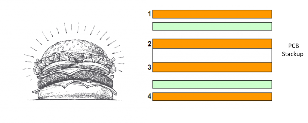
A PCB stack-up is the construction of a multilayer PCB in sequential order. A stack-up consists of cores, prepregs, and copper foils. Generally, stack-ups are symmetrical. The majority of the products fall under 62-mil board thickness.
What materials are used in circuit boards?
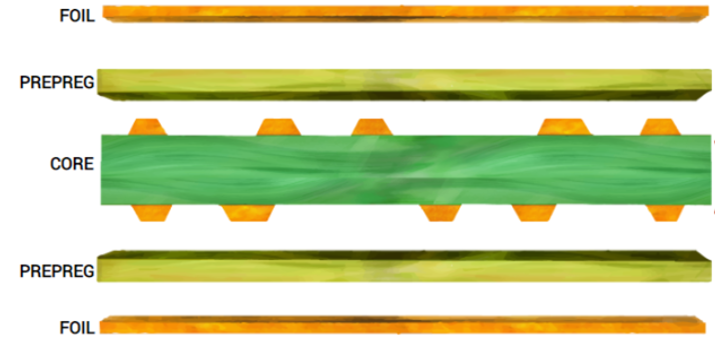
A printed circuit board is manufactured using the following 3 items:
- Prepreg: B Stage Material that is tacky and allows bonding of different laminates or foils
- Copper foil: Serves as a conductor in PCBs.
- Copper Clad Laminates (Core): Made of prepregs and copper foils that have been laminated and cured.
Basic properties of the dielectric materials
We know that PCB laminates are made of dielectric materials. While choosing laminates, we need to consider various properties of the dielectric material used. They are:
| Thermal properties | Electrical properties |
|---|---|
| Glass transition temperature (Tg) | Dielectric constant (Dk) |
| Decomposition temperature (Td) | Loss tangent or dissipation factor (Tan δ or Df) |
| Thermal conductivity (k) | |
| Coefficient of Thermal Expansion (CTE) |
Thermal properties:
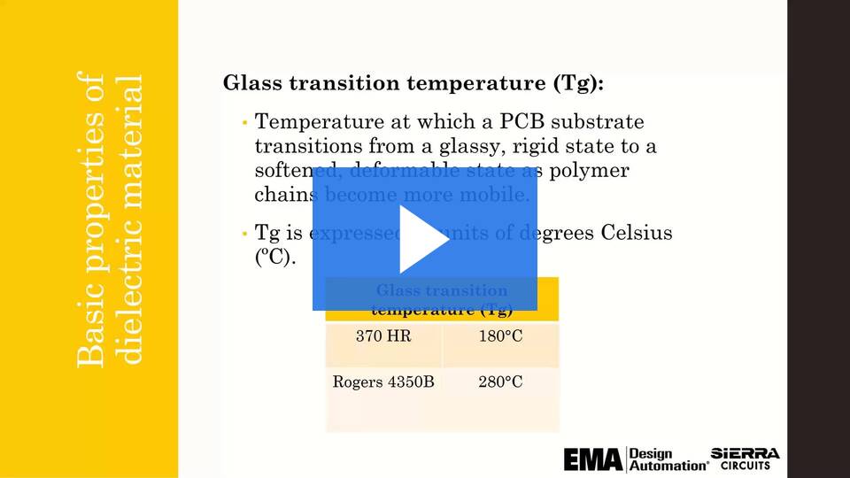
Glass transition temperature (Tg): Glass transition temperature, or Tg, is the temperature range in which a substrate transitions from a glassy, rigid state to a softened, deformable state as polymer chains become more mobile. When the material cools back down, its properties return to their original states. Tg is expressed in units of degrees Celsius (°C).
Decomposition Temperature (Td): Decomposition temperature, or Td, is the temperature at which a PCB material chemically decomposes (the material loses at least 5% of mass). Like Tg, Td is expressed in units of degrees Celsius (°C).
Thermal conductivity (K): Thermal conductivity, or k, is the property of a material to conduct heat; low thermal conductivity means low heat transfer while high conductivity means high heat transfer. The measure of the rate of heat transfer is expressed in watts per meter per degree Celsius (W/M °C).
Coefficient of Thermal Expansion (CTE): The coefficient of thermal expansion, or CTE, is the rate of expansion of a PCB material as it heats up. CTE is expressed in parts per million (ppm) expanded for every degree Celsius that it is heated. As a material’s temperature rises past Tg, the CTE will rise as well. The CTE of a substrate is usually much higher than copper, which can cause interconnection issues as a PCB is heated.
Electrical properties:
Dielectric constant (Er or Dk): Considering the dielectric constant of a material is important for signal integrity and impedance considerations, which are critical factors for high-frequency electrical performance. The Er for most PCB materials is in the range of 2.5 to 4.5.
The values in the datasheets are only valid for a specific (usually 50%) resin content percentage in the material. Actual resin percentage in a core or prepreg varies with composition and Dk changes due to that. Copper percentage and press out the thickness of prepreg will finally decide the dielectric height. The dielectric constant generally decreases with an increase in frequency.
Loss tangent (tanδ) or dissipation factor (Df): The loss tangent or dissipation factor is the tangent of the phase angle between the resistive and reactive currents in the dielectric. The dielectric loss increases with increasing values of Df. Low values of Df result in a “fast” substrate while large values result in a “slow” substrate. Df increases slightly with frequency; for high-frequency materials with very low values of Df, it has a very low variation with frequency. Values range from 0.001 to 0.030.
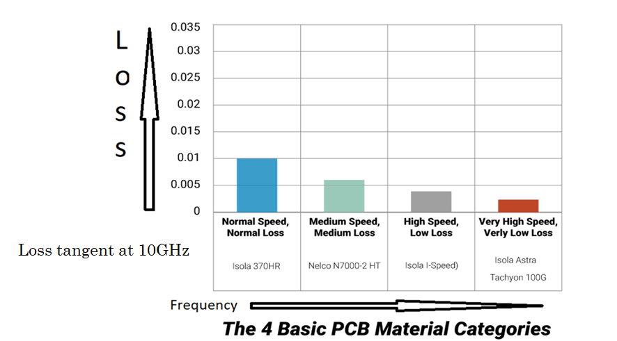
PCB material selection: The basic categories
The basic PCB material categories are:
- Normal speed and loss
- Medium speed and loss
- High speed and low loss
- Very high speed and very low loss (RF/microwave)
Normal speed and loss: Normal-speed materials are the most common PCB materials—the FR-4 family. Their dielectric constant (Dk) versus frequency response is not very flat and they have a higher dielectric loss. Therefore, their suitability is limited to a few GHz digital/analog applications. An example of this material is Isola 370HR.
Medium speed and loss: Medium-speed materials have a flatter Dk versus frequency response curve, and have a dielectric loss of about half that for normal speed materials. These are suitable for up to ~10GHz. An example of this material is Nelco N7000-2 HT.
High speed and low loss: These materials also have flatter Dk versus frequency response curves and low dielectric loss. They also generate less unwanted electrical noise compared to other materials. An example of this material is Isola I-Speed.
Very high speed and very low loss (RF/microwave): Materials for RF/microwave applications have the flattest Dk versus frequency response and the least dielectric loss. They are suitable for up to ~20GHz applications. An example of this material is Isola I-Tera MT40 and Tachyon 100G.
Sierra Circuits application specific PCB materials
| Board type | Recommended materials |
|---|---|
| Standard FR-4 lead free boards | Isola 370 HR Ventec VT47 |
| High speed materials with processing similar to standard FR-4 | Isola FR408HR Isola I-Speed Isola I-Tera Isola Astra MT77 Isola Tachyon 100G |
| Ceramic-reinforced boards | Rogers RO4350 B Rogers TTM Rogers RO4003 Rogers RO4230 |
| Standard polyimide boards | Isola P95 Nelco N7000-2HT |
| Advanced Teflon boards | Rogers RO3000 Series Rogers RT/DUROID Series Rogers ULTRALAM 2000 |
| Standard flex boards | DuPont Pyralux AP DuPont Pyralux LF DuPont Pyralux FR |
| Boards that require high thermal conductivity | Thermagon 88 Laird IMPCB |
Signal loss and operating frequency
The PCB material can affect the signal integrity of your high-frequency circuits. You can minimize attenuation on your board by choosing the right PCB substrates and copper foil. These two materials play a very important role when it comes to signal loss in your PCB. Signal loss comprises dielectric loss and copper loss.
Dielectric loss
Dielectric materials are made up of polarized molecules. These molecules vibrate in the electric fields generated by the time-varying signals on the signal traces. This heats up the dielectric and results in the dielectric loss part of signal losses. This signal loss increases with frequency. Signal loss can be minimized by using a material that has a lower dissipation factor. The higher the frequency, the more will be the loss in any given material. This is due to the changing electromagnetic field causing the molecules in the dielectric material to vibrate. The faster the molecules vibrate, the higher the loss.
Copper loss
Copper loss is essentially associated with the current that flows through the conductors. Electrons may not always flow through the centers of the conductors. If a copper trace is finished with nickel, most of the current might flow through that nickel layer. The skin-effect loss gets larger as frequencies go up. This can be compensated by increasing the width of the traces which in turn creates a larger surface area. Wider trace will always have lower skin effect loss. Copper foil-dielectric toothy interface profile increases the effective length and thus increases the copper loss. It is always recommended to use the low profile or very low profile copper.
Correlation between signal loss and operating frequency
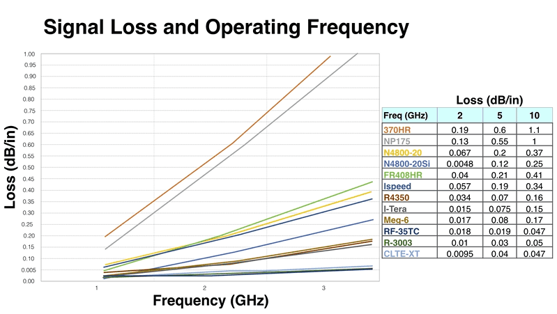
As you can see from the graph above, there’s a direct correlation between signal loss and frequency. At the same time, we can also see that certain materials are less lossy than others. Signal loss or attenuation increases with frequency. The graph shows which materials could possibly perform better electrically at higher speeds.
For better PCB material selection, the below chart classifies the essential materials into various buckets based on the signal loss properties.

On the left, we have materials like FR-4. These are your standard and simple to process, everyday materials that can be used in any application. But they are also the lossiest laminates. It can also have a plethora of other electrical and mechanical issues. Materials like Isola I-speed, Isola Astra, and Tachyon exhibit low loss at high frequencies.
Copper foil selection
Below are a few properties that we need to consider while selecting copper foil:
- Copper thickness: Typical thickness varies from 0.25 oz (0.3 mils) to 5 oz (7 mils).
- Copper purity: It is the percentage of copper found in the copper foil. Electronic grade copper foil has a purity of around 99.7%.
- Copper-dielectric interface Profile: Low profile has lower signal copper losses at high frequencies.
Copper foil types
Electro-deposited copper: This type of copper has a vertical grain structure and a rougher surface. Electro-deposited copper is typically used in rigid PCBs.
Rolled copper: A type of copper, made very thin by processing between heavy rollers, extensively used to produce flexible PCBs. Rolled copper has a horizontal grain structure and a smoother surface which makes them ideal for rigid-flex and flex PCBs.
PCB material selection best practices
- Match coefficient of thermal expansion (CTE): CTE is the most critical thermal characteristic for substrates. If the components of the substrates have different CTE, they may expand at different rates during the fabrication process.
- Opt for tight substrate weave: The Dk distribution in tight substrate weave will be even.
- Avoid FR (flame retardant) 4 for high-frequency applications: This is due to its high dielectric loss and steeper Dk versus frequency response curve. (For frequencies less than 1 GHz).
- Use lower moisture absorption materials: Moisture absorption is the ability of a PCB material (copper in this case) to resist water absorption when immersed in water. It is given by percentage increase in weight of a PCB material due to water absorption under controlled conditions as per standard test methods. Most materials have moisture absorption values in the range of 0.01% to 0.20%.
- Always use CAF-resistant materials: Conductive anodic filament (CAF) is a metallic filament that forms from an electrochemical migration process and is known to cause PCB failures. Using CAF-resistant materials is one of the most effective ways to prevent CAF formation and failure.
To learn how to address voiding, CAF, and electromigration in high-voltage boards, see how to select components and materials for power electronics PCBs.
Significance of PCB stack-up and example stack-ups
- An accurately stacked PCB will reduce electromagnetic emissions, crosstalk, and improve the signal integrity.
- It controls the impedance of traces.
- Reduces the size of the PCB.
- Reduces the routing density.
- Provides low noise ground and power planes.
- Reduces the resistivity of the ground and power planes.
Example stack-ups
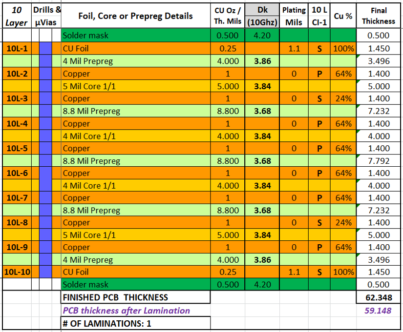
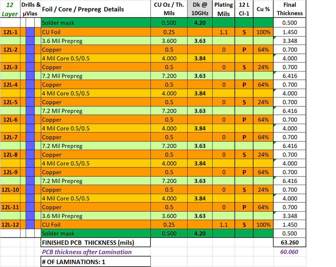
Typical 12 layer PCB stack-up
HDI boards and key considerations
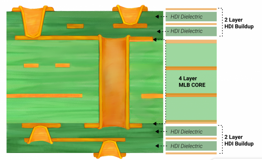
High-density interconnects (HDI) PCBs are the boards with a higher wiring density per unit area than conventional PCBs. Some important features of HDI boards are:
- Fine lines/spaces less than or equal to 100µm.
- Microvias less than or equal to 150µm.
- Capture pads less than 400µm
- Capture pad density greater than 20 pads per centimeter square.
HDI PCB Design Guide
5 Chapters - 52 Pages - 60 Minute ReadWhat's Inside:
- Planning your stack-up and microvia structure
- Choosing the right materials
- Signal integrity and controlled impedance in HDI
- Manufacturing considerations for higher yields
Download Now
PCB material selection for quality HDI boards
Dimensional stability: The material should be dimensionally stable; this also applies to the non-HDI PCBs as well. All materials shrink and stretch to some extent during manufacturing processes, and patterning must be scaled to compensate, which is not an issue provided the material movement is predictable.
Machinability: The material must be easily machinable. For HDI that means it can be laser drilled (Vaporization) without problems. Highly concentrated energy is directed in a focused beam on a specific area, which is absorbed by the material until it vaporizes.
Epoxy resin is the most commonly used thermosetting resin and is the backbone of the industry. Thanks to its relatively low cost, excellent adhesion (to the metal foils as well as to itself), and good thermal, mechanical, and electrical properties. Make sure the chosen material is suitable for sequential laminations. Sierra Circuits recommends I-Speed and I-TeraMT40 materials for HDI PCBs.
OhmegaPly material is one of the most reliable materials that can be used in HDI boards.
Files/data that a PCB manufacturer expects from a designer
Below are few production files expected by a PCB manufacturer from a designer.
Gerbers: Gerber files are a set of files that contain production information of each layer of a PCB. The top and bottom silkscreen, top and bottom paste mask, top and bottom solder mask. Top and bottom assembly layers should be mentioned in the fab details.
ODB++: ODB++ is an intelligent format. A single ODB++ file or directory contains all the information required to define a PCB layer. . A single ODB++ file or directory contains all the information required to define a PCB layer. This file format offers a stable framework for the required data. An ODB++ file doesn’t ensure that the given data is sufficient to manufacture the design but it allows the designer to combine all the data and perform the required checks for manufacturability and reliability.
IPC-2581: IPC-2581 is a universal PCB assembly and manufacturing standard for data definition and transition methodology. IPC-2581 can include a large number of files within a single XML file.
Fab drawing Outline drill drawing: The fab drawings give the manufacturing details of the PCB, this includes board dimensions, drill details, class of fabrication (class 2, class 3), and stack-up details. Fabrication drawings are sent in PDF format to manufacturers and all designing tools support the function that exports PDF-formatted fab drawings.
NC drill: An NC drill file gives information about all the holes required in the board. It will serve as an input to the drill machine to drill the required holes on the board.
Pick and place file: Pick and place files are used by the machine to identify the location of the various components on the board using coordinates.
IPC-356 netlist file: IPC-356 netlist files have information about the connections between various components. Once you create your netlist make sure that it matches your schematic netlist.
Bill of materials: BOM or bill of materials contains the list of all components and its specification required for the fabrication of the design. Designers can generate customized BOM from their designing software that lists all of the footprints of the components in an Excel spreadsheet. These BOMs are used as a reference for the fabricators to assemble the components in the correct order by referring to the footprints and designator.
Proper PCB material selection is important since materials will affect the electrical performance of the signal traces. Following the guidelines provided in this PCB material selection webinar enables you to choose the best possible materials for your design.
PCB Material Design Guide
9 Chapters - 30 Pages - 40 Minute ReadWhat's Inside:
- Basic properties of the dielectric material to be considered
- Signal loss in PCB substrates
- Copper foil selection
- Key considerations for choosing PCB materials
Download Now


