Contents

On-demand webinar
How Good is My Shield? An Introduction to Transfer Impedance and Shielding Effectiveness
by Karen Burnham
With the rapid advancements in AI and IoT technologies, modern circuit designs demand careful attention to electrical, mechanical, and thermal factors.
Engineers face many PCB design challenges such as maintaining signal integrity, managing heat dissipation, and ensuring structural reliability while creating prototypes.
In this article, you’ll learn the 5 common PCB design challenges and practical solutions to tackle them.
Highlights:
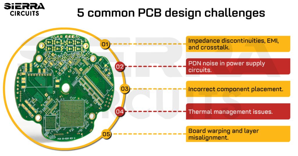
Common obstacles seen in PCB design:
- Impedance discontinuities, EMI, and crosstalk.
- PDN noise in power supply circuits.
- Incorrect component placement and part overlapping.
- Thermal management challenges.
- Board warping and layer misalignment.
Challenge #1: Impedance discontinuities, EMI, and crosstalk
Signal integrity issues are often caused by abrupt changes in trace width, poor routing practices, improper grounding, and inadequate spacing between high-speed signal traces. Here, we will take you through the techniques a signal integrity engineer can use to avoid these PCB design challenges.
7 techniques to address impedance discontinuities
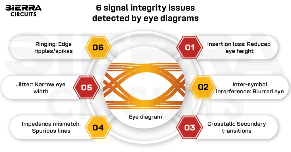
When impedance is inconsistent in a circuit, signals can reflect toward the source and interfere with the transmitting pulses. This can cause oscillating voltage or current, leading to PCB ringing, overshooting (the signal exceeds its steady state), and undershooting (the signal is lower than its final value).
Impedance mismatches might generally occur at:
1. Unterminated signal lines.
2. Intersection points of a signal with a via or connector pin.
3. Abrupt trace width changes during layer transition.
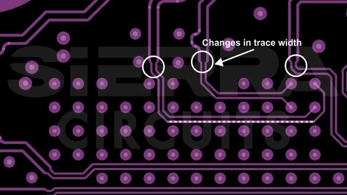
4. Unwanted via and trace stubs.
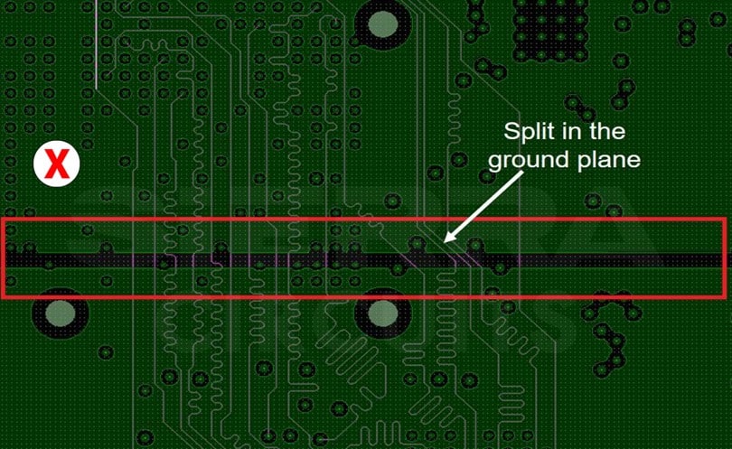
5. Splits in the return path or reference plane, as shown in the below image.
Follow these guidelines to achieve uniform impedance in your PCB layout:
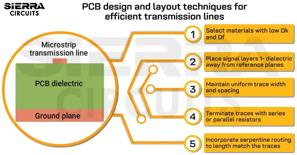
1. Ensure consistent trace width, thickness, and spacing along the signal transmission path.
2. Route traces in a daisy chain fashion. A daisy chain trace routing refers to connecting components in series, one after the other, rather than multi-drop branches.

3. Place a damping resistor near the source to reduce the reflected signal amplitude and prevent it from interfering with the original signal.
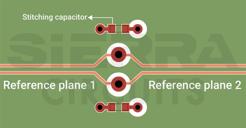
4. When routing signals over two reference planes, incorporate stitching capacitors to achieve a continuous signal return path.
5. Incorporate PCB trace termination techniques to match the transmission line impedance with the impedance of the connected components. Here are the 2 common termination approaches:
a. Series termination: Place a resistor in series between the driver and the transmission line. The resistor should be close to the source to match the driver’s impedance with the trace characteristic impedance.

b. Parallel termination: Place a termination resistor parallel to the receiver to reduce signal reflections at the load end.

6. When a signal changes its reference plane, place transition vias close to the signal vias. These vias provide direct routes for signals to switch between different reference planes.
7. Keep trace lengths as short as possible, especially in high-frequency circuits where even small inductances can cause substantial issues. Long traces can act as antennas, increasing inductance and causing reflections.
For more high-speed design rules, download our eBook.

High-Speed PCB Design Guide
8 Chapters - 115 Pages - 150 Minute ReadWhat's Inside:
- Explanations of signal integrity issues
- Understanding transmission lines and controlled impedance
- Selection process of high-speed PCB materials
- High-speed layout guidelines
Download Now
At Sierra Circuits, we can build PCBs with ±5% impedance tolerance. We add impedance test coupons to each panel and validate the impedance to ensure it matches your requirements. These test coupons replicate the trace structure and layer stack-up of the actual PCB.

See our controlled impedance capabilities to learn more.
5 layout strategies to reduce EMI
Electromagnetic interference occurs when energy is unintentionally radiated or conducted from an electronic device. EMI can originate from various components, including traces, vias, connectors, and cables.
This PCB design challenge is primarily caused by:
- Electromagnetic emissions: Energy radiated from an electronic device. This radiation can be of 2 types:
- Radiated emission: These are emissions in the form of EM waves radiated into free space from a source. A few instances of radiated emissions are:
- High-speed switching in digital circuits, radiating EM energy at harmonics of the switching frequency.
- Unshielded high-speed cables (like HDMI or USB cables), act as antennas.
- Traces on a PCB carrying high-frequency signals with no solid ground return path.
- Conducted emission: These are unwanted signals that propagate through conductors, such as power lines, ground lines, and signal cables. For instance,
- Power supply noise is coupled to the main power line.
- High-frequency noise is conducted through improperly filtered signal lines or power traces.
- Radiated emission: These are emissions in the form of EM waves radiated into free space from a source. A few instances of radiated emissions are:
- Susceptibility to EM radiation: The tendency of an electronic device to be affected by external electromagnetic energy.
See 7 tips and PCB design guidelines for EMI and EMC.
Incorporate these techniques to avert EMI in your designs:
- Employ a Faraday cage, a continuous copper fill around sensitive circuitry. It is a continuous, conductive enclosure (typically copper) that surrounds sensitive circuitry. It blocks electromagnetic fields from escaping the circuit and prevents external EM fields from hindering the circuit. Make sure the shield is properly grounded to prevent resonance and maximize EMI suppression.
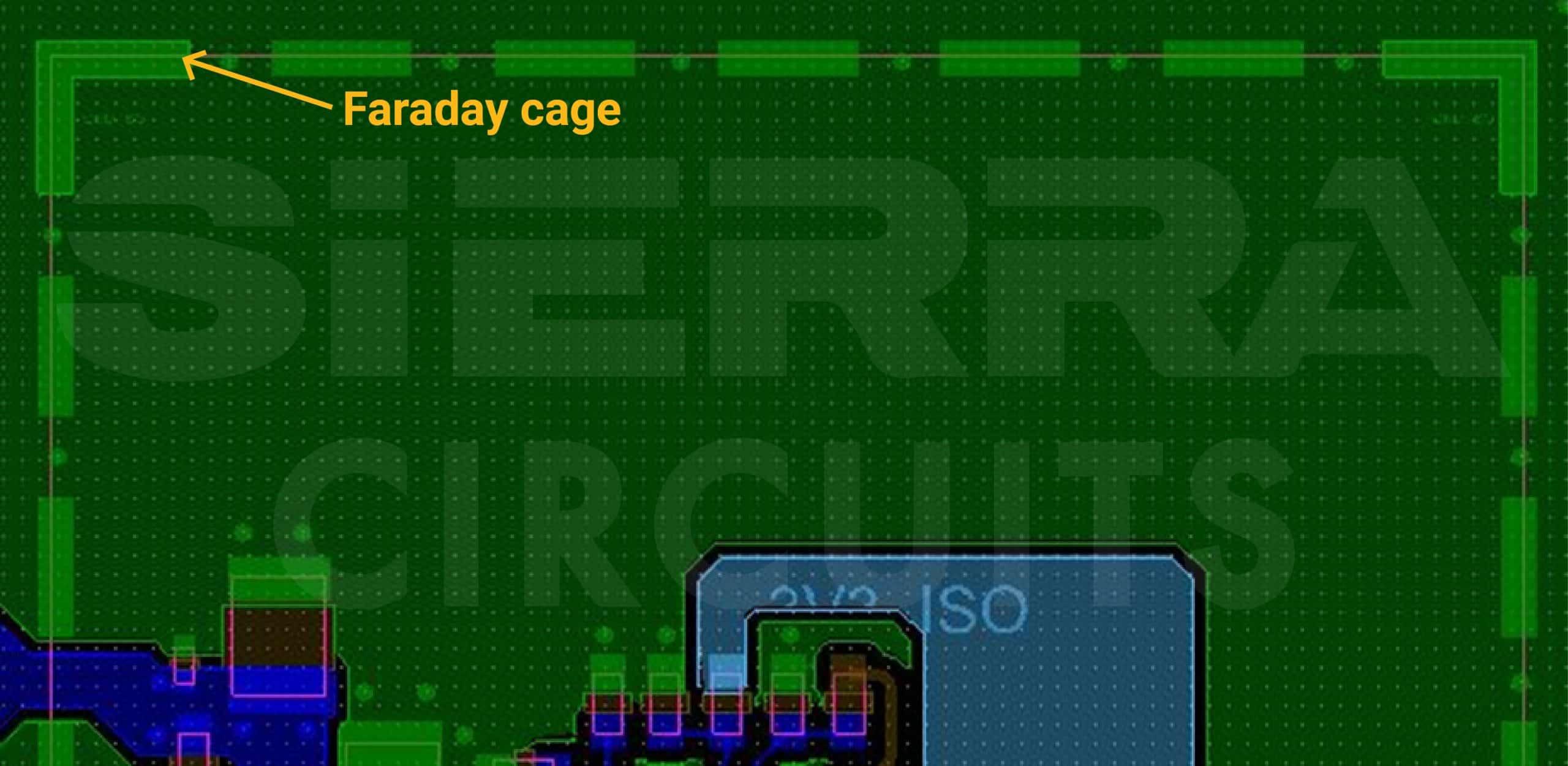
Faraday cage shields sensitive circuitry from external EM radiation. - Avoid discontinuities in the ground plane. Splits, gaps, or voids in the ground plane can act as unintended antennas that radiate or pick up electromagnetic energy. High-frequency signals with poor return paths are especially problematic.
- Shield cables with conductive material that acts as a barrier to electromagnetic fields. Shielded cables use a conductive layer (braid, foil, or both) around the signal-carrying wires. The shield blocks electromagnetic energy and reduces interference. Always, ground the shield at one or both ends, depending on the application (single-point grounding for low-frequency signals and multi-point grounding for high-frequency signals).
- Use copper pours connected to the ground plane. This provides additional shielding and helps with heat dissipation. The spacing between a high-speed/RF trace and ground pours should be 1.5 to 2 times the trace width. Ensure ground pours do not create isolated ground islands, which can act as unintended antennas and lead to challenges in PCB designs.
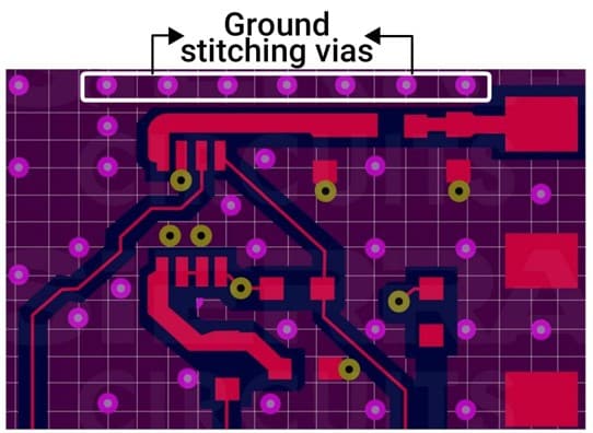
- Implement via stitching to provide multiple low-impedance paths to the ground. Via stitching involves placing multiple vias along the edges of a ground plane or around critical signal traces. This technique minimizes the potential for radiation and noise coupling. The spacing between two adjacent vias should typically range between λ/20 and λ/10, where λ is the signal’s operating wavelength. Adhering to this guideline helps ensure optimal isolation and reduces unwanted radiation at high frequencies.
The above are the strategies generally used by professional designers to minimize EMI. How do you deal with EMI? Share your insights in the comments section at the bottom. We’d love to learn more from you.
5 best practices to reduce crosstalk in your circuit boards
Crosstalk in PCBs occurs when two adjacent conductors are close together, allowing energy to couple from the aggressor to the victim trace.
When current flows through a conductor, it generates a magnetic field around it. If another trace runs parallel to the first one, the changing magnetic field induces a voltage in the adjacent trace.
This effect is more pronounced when the traces are close together. High-speed digital signals, clock lines, and analog signals are particularly susceptible to crosstalk.
To minimize crosstalk and ensure reliable high-speed signal transmission, stick to the following 5 guidelines:
1. Ensure sufficient spacing between adjacent signal traces. The recommended clearance is typically 3 to 5 times the trace width to minimize electric field coupling.
2. Place signal planes close to ground planes (preferably 1 dielectric away). Ground planes act as shields, providing a low-impedance return path.
3. Avoid running RF traces parallel to other signal traces to prevent coupling. Running traces in parallel increases electromagnetic interference, particularly at high frequencies.
RF & Microwave Design Guide
8 Chapters - 44 Pages - 60 Minute ReadWhat's Inside:
- Basics of RF and microwave board design
- Choosing RF materials
- Trace, grounding, via, and stack-up design
- Component selection and placement
- Testing and isolation requirements to avoid interference
Download Now
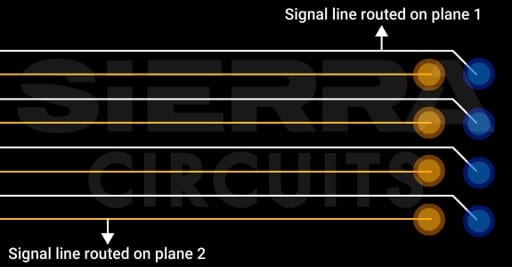
4. When routing critical signals on two adjacent planes, ensure there is no overlap between the signals. Overlapping high-speed or sensitive signal traces (e.g., clock lines, data buses) on adjacent planes increases the likelihood of field coupling.
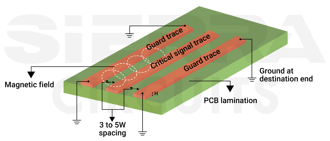
5. Add guard traces next to critical signal lines. Determine which signal traces are most susceptible to crosstalk and place guard traces parallel to and surrounding the critical signal traces. Keep a consistent distance of 3W to 5W between the guard traces and the critical signal traces.
Challenge #2: PDN noise in power supply circuits
Power integrity ensures the PDN provides stable and noise-free power to all components on the PCB, which is critical for high-speed designs and sensitive electronics.
4 common sources of PDN noise
- Voltage drops occur when power traces have insufficient width and are too resistive to handle high current demand, especially during transient spikes. In high-current PDNs, a small voltage drop of 100 mV on a 1.2 V supply can cause critical components to fail.
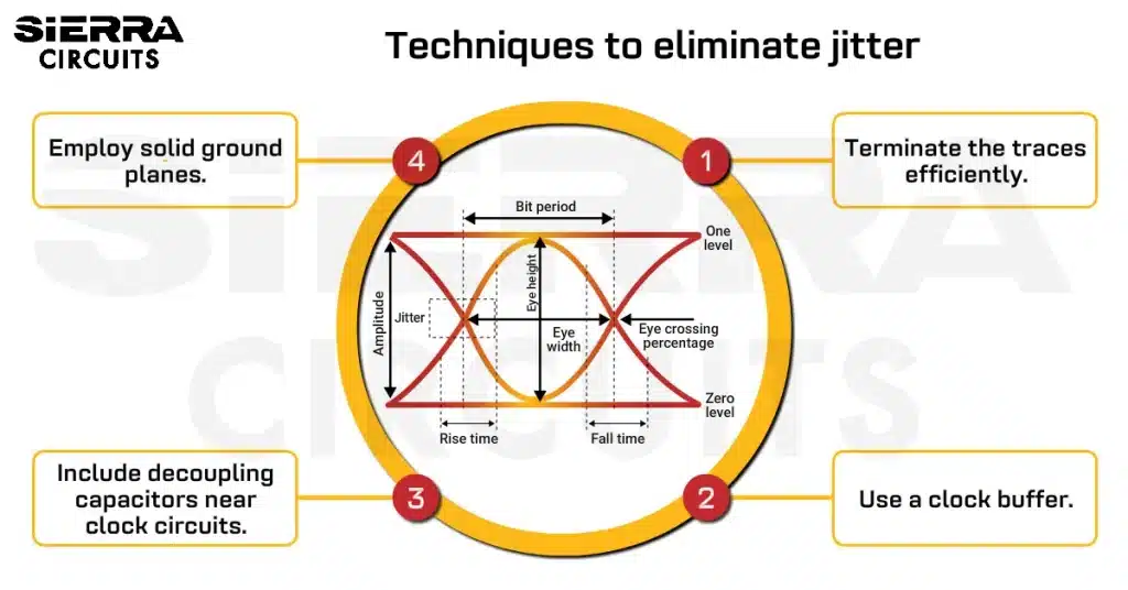
- Switching noise is caused by the rapid switching of power supplies (e.g., DC-DC converters or VRMs), which introduces high-frequency ripple and transient noise on the power rails. Sensitive ICs, especially microprocessors or high-speed digital devices, may experience jitter in clock signals. High ripple can cause data corruption in digital interfaces.
- High resistance in narrow traces leads to power losses. Over time, heat accumulation can cause:
- Trace overheating and degradation.
- Damage to components.
- Thermal runaway in power-intensive designs.
- When power is not distributed uniformly, some components may receive insufficient current while others may draw excess current. Underpowered components can malfunction or fail to operate. Overloaded components may overheat, shortening their lifespan and reducing system reliability.
4 tips for designing efficient power supply in your PCBs
- Use dedicated power and ground planes stacked closely in a multilayer PCB. This reduces parasitic inductance and ensures a low-impedance return path, minimizing power noise and improving signal integrity.
- Incorporate bypass capacitors to nullify low-frequency ripple in the power supply.
- Implement via-in-pad structures for IC power pins. They provide a direct, low-inductance connection to internal planes, improving current delivery.
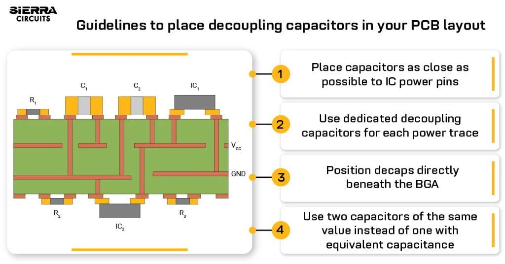
- Place multiple decoupling capacitors (e.g., 0.1 µF and 10 µF) near the power pins of ICs. These capacitors filter high-frequency noise and provide local charge during transient conditions. Place capacitors as close as possible to the IC power pins to reduce parasitic inductance. Use low-ESR capacitors for improved performance at high frequencies.
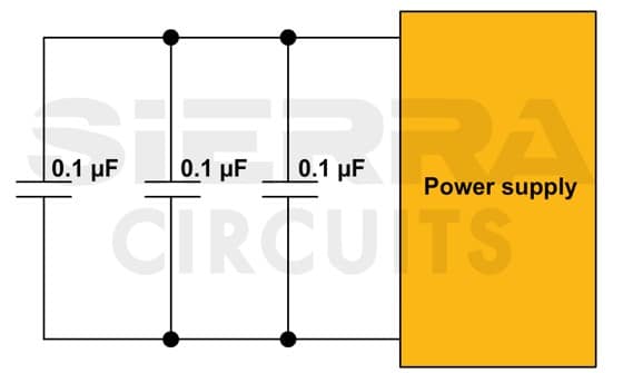
Multiple decoupling capacitors in parallel with a power supply to prevent PDN noise.
Challenge #3: Incorrect component placement and overlapping
Component placement directly influences a PCB’s electrical performance, heat dissipation, manufacturability, and reliability. Inefficient part placement complicates routing and can result in noise issues, signal integrity problems, and thermal inefficiencies.
Below, you’ll learn the PCB design challenges in part placement and provide solutions to avoid them.
Why component placement matters
- Inefficient placement increases trace lengths, leading to signal integrity, timing, and power distribution issues. It can also result in denser routing, making the layout harder to optimize.
- Poor placement can make testing points, debugging interfaces, or key components hard to access, complicating troubleshooting and repair.
- Insufficient component-to-component clearances cause part overlapping and solder bridges. Components too close to the traces can result in shorts due to solder wicking. Additionally, parts placed close to the board edge are more susceptible to damage during handling and reflow soldering.
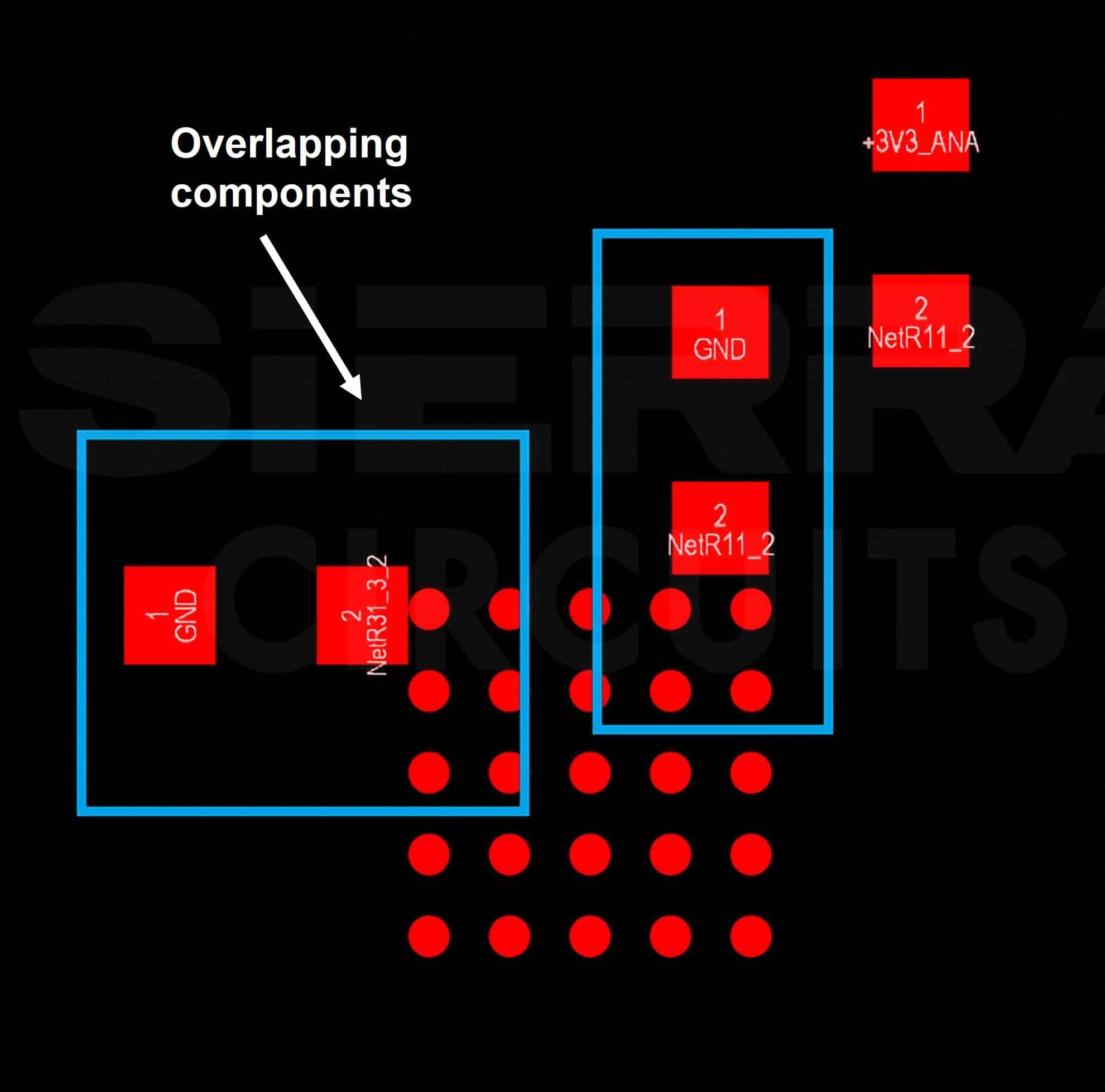
Overlapping components lead to assembly issues.
6 best techniques for effective component placement
1. Group components based on their function (e.g., power regulation, analog signals, high-speed signals). This reduces routing complexity and improves signal integrity.
2. Standardize the orientation of similar electronic components (e.g., ICs, diodes) to simplify assembly and inspection. Align all IC pin 1 markings in the same direction. Consistent orientation simplifies automated assembly, inspection, and repair.
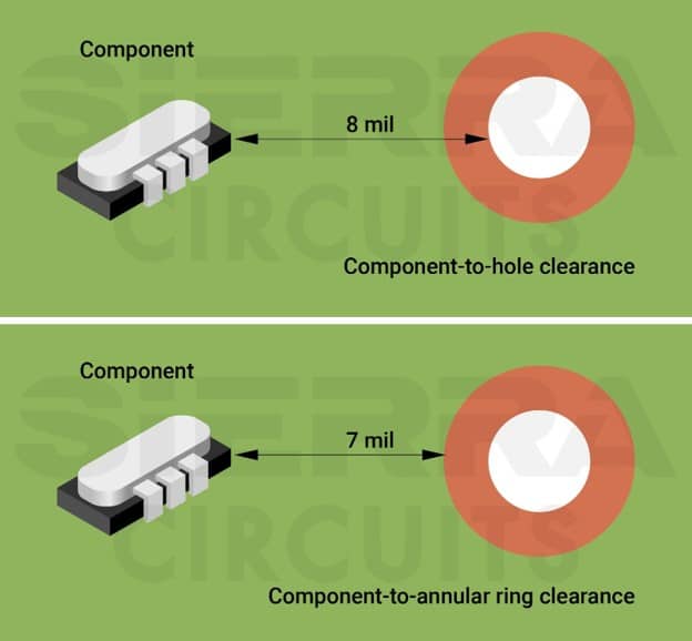
3. Incorporate at least 8 mil part-to-hole distance. The spacing between the component pad to the annular ring edge should be a minimum of 7 mil. Components placed close to the traces can result in shorts due to solder wicking.
4. Position high-speed components such as processors, memory, and high-speed transceivers near each other. This minimizes trace lengths, reducing signal propagation delay and ensuring signal integrity.
5. Include clear component outlines and reference centroids. Maintain a 1:1 ratio between solder mask openings and pads. This reduces the risk of component misalignment. Misaligned components can result in soldering issues and tombstoning.
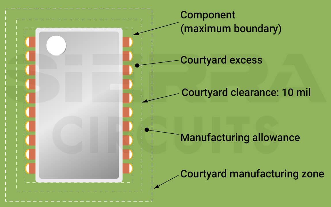
6. Have at least 10 mil of courtyard clearance for all the components. Sensitive devices like BGA should have a clearance of 39 mil. Connectors, crystals, and canned capacitors need a minimum of 20 mil clearance.
Challenge #4: Thermal management challenges in PCB designs
Effective PCB thermal management is essential to ensure the long-term reliability of your board. Excessive heat can degrade components over time, reduce operational efficiency, and even lead to catastrophic failures. As a product developer, you might face these obstacles when it comes to dissipating heat from your device:
- Prolonged exposure to elevated temperatures can degrade electronic components over time, shortening their operational lifespan. Many electronic components have maximum temperature ratings (e.g., junction temperature for semiconductors), and exceeding these thresholds can lead to permanent damage.
- In power electronics, excessive heating can result in a self-reinforcing cycle called thermal runaway. As components heat, their electrical properties change, leading to increased current draw. This, in turn, generates more heat, further accelerating the temperature rise. Without proper heat dissipation, this can result in component or system failure.
- PCBs undergo heating and cooling cycles during operation. Each cycle causes the expansion and contraction of PCB materials due to thermal stress. Over time, this repeated stress can:
- Weaken solder joints, causing fatigue cracks.
- Lead to microfractures in traces or vias, resulting in electrical discontinuities and failures.
- Poor heat dissipation leads to localized hotspots, which increase the electrical resistance of copper traces. As resistance rises, voltage drops occur, reducing efficiency and power delivery capability. These localized hotspots can exacerbate thermal issues, leading to cascading failures.
6 design techniques for effective heat dissipation
- Use materials with a high glass transition temperature (Tg > 180°C) to ensure stability under high thermal loads. High-Tg PCBs resist deformation, maintain dimensional stability, and preserve electrical insulation properties at elevated temperatures.
- Different materials (e.g., copper, FR4, solder joints) expand at different rates during thermal cycling. High-CTE mismatches create mechanical stress, leading to delamination, solder joint cracking, and long-term fatigue. Incorporate materials with a low coefficient of thermal expansion (CTE < 70 ppm/°C) to minimize expansion mismatches between layers and components, reducing the likelihood of mechanical stress or delamination.
- Increase copper thickness (e.g., 3–5 oz per square foot) to reduce trace resistance and improve heat conduction. This is particularly beneficial for addressing PCB design challenges in power delivery.
- Place multiple thermal vias under or near high-power components to transfer heat from the surface layer to internal or external heat sinks. These vias transfer heat from the surface layers to internal ground planes or external heat sinks. They improve vertical heat conduction through the PCB. Use multiple vias to maximize heat transfer. For high-power components, consider via-in-pad structures for better thermal contact.
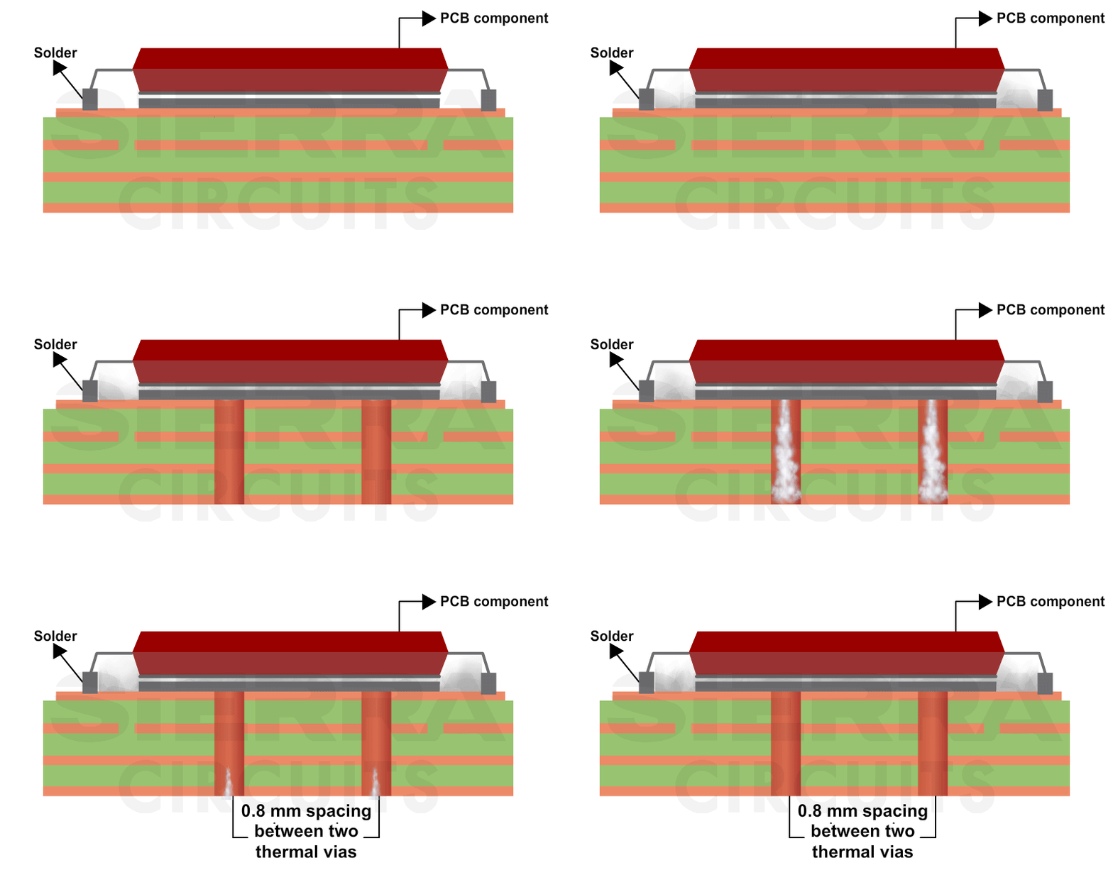
Position thermal vias close to heat-generating components to create an efficient thermal path and minimize thermal resistance. Include thermal vias directly under the thermal solder pads for circuit boards with more than 0.7 mm (28 mil) thickness. Choose a 0.3 mm via diameter and 0.8 mm via-to-via spacing. This balances mechanical stability and thermal performance without compromising board integrity.
- Add external heat sinks or active cooling fans to dissipate heat efficiently from critical areas, especially in densely packed or high-power designs. Blocked paths can trap heat and cause components to exceed their temperature limits. It occurs due to dense component placement and if parts are placed directly over heatsinks.
- Ensure sufficient airflow over the heatsinks to avoid hotspots. Locate high-power components centrally on the PCB to distribute heat more uniformly. This reduces localized hotspots and ensures a balanced thermal load across the board.
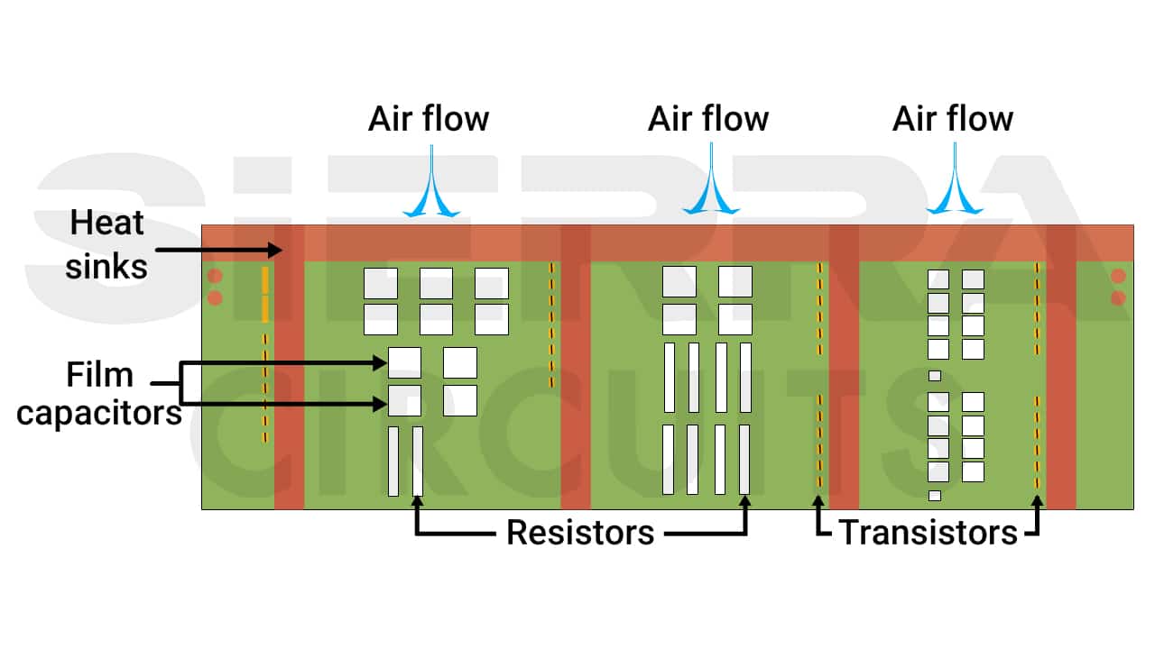
Ensure sufficient airflow from heat sinks for efficient heat dissipation. - Have wide power traces to reduce resistance, and improve current-carrying capacity, and heat dissipation. Use Sierra Circuits’ Trace Width, Temperature Rise, and Current Capacity Calculator to optimize trace width based on your current requirements and ambient temperature.
Challenge #5: Board warping and layer misalignment in PCB designs
In circuit designs, mechanical constraints such as warping, microcracks, bowing, and component stress might cause dimensional changes, and layer misalignment.
These PCB design challenges become critical for circuits operating in high-temperature or harsh environments, where even a slight bend or crack can compromise the board’s structural integrity and overall reliability.
Addressing these issues early in the design and manufacturing process is essential to ensure robust performance under demanding conditions.
Some of the common mechanical hurdles include:
- Board materials, such as copper and substrate layers, have different coefficients of thermal expansion (CTE). During temperature fluctuations, these materials expand or contract at different rates, leading to the delamination of layers or the formation of micro-cracks in copper traces.
- Thin or oversized PCBs are more prone to bending, bowing, or warping during assembly or operation. These deformations might cause component misalignment or physical damage to traces.
- Printed boards used in automotive, aerospace, and industrial applications are subjected to constant mechanical vibrations. This can lead to:
- Solder joint fatigue.
- Component detachment.
- Cracks in traces or vias.
- Physical stress during PCB assembly might damage solder joints, compromising reliability. Misaligned connectors can also apply shear force or torque to the board during mating cycles.
6 tips to avoid mechanical damage to your PCBs
- Incorporate features like rounded corners, curved traces, and fillets to evenly distribute mechanical stress and reduce structural challenges in PCB design.
- Align components with similar dimensions on the same orientation to minimize stress during handling, assembly, and operation.
- Apply conformal coatings to shield the PCB from:
- Moisture can cause corrosion or short circuits.
- Vibration that can loosen solder joints.
- Temperature fluctuations that exacerbate mechanical stress.
- Add stiffeners or metal backing for added support in flexible PCBs or thin designs.
- Use finite element analysis (FEA) tools to simulate:
- Thermal cycles and predict delamination risks.
- Mechanical stress is caused by bending, vibration, or assembly forces.
- Use durable materials such as FR-4 with fiberglass reinforcement or high-performance substrates like polyimide for high-temperature environments to prevent this PCB design challenge.
For guidelines on designing a PCB prototype, see building a PCB prototype from scratch: A designer’s guide.
Key takeaways:
- Ensure consistent trace width, thickness, and spacing along the signal transmission path to achieve uniform impedance.
- Employ a Faraday cage to block EM radiation.
- Have at least 3 to 5 times the trace width to minimize crosstalk.
- Incorporate wide traces to facilitate heat dissipation.
- Place multiple decoupling capacitors (e.g., 0.1 µF and 10 µF) near the power pins of ICs.
- Group components based on their function.
- Opt for materials with a low coefficient of thermal expansion (CTE) to reduce mismatched expansion rates between layers.
Designing a PCB is a balancing act that requires addressing hurdles across multiple disciplines. From signal integrity to thermal management, power distribution, and structural reliability, each factor plays a vital role in ensuring optimal performance.
Proactively tackling these PCB design challenges through strategic planning, precise layout techniques, and the right material choices ensures your circuit board meets both functional and durability requirements. By integrating these best practices into your design process, you can deliver reliable, high-performance boards tailored to the demands of modern electronics.
Need answers to your prototype design questions? Post your queries on SierraConnect. Our PCB experts will answer them.








Start the discussion at sierraconnect.protoexpress.com