Contents

On-demand webinar
How Good is My Shield? An Introduction to Transfer Impedance and Shielding Effectiveness
by Karen Burnham
OhmeagPly (resistive conductive material) and TCR material (thin-film resistor foil) follow the embedded passives technology (EPT), which manufactures passive components such as resistors and capacitors into the substrate of PCBs during the fabrication process of a bare board.
These materials are more influential, highly reliable, efficient, and functional for high-speed applications. In this article, you’ll learn the basics of processing OhmegaPly material.
What is an OhmegaPly material?
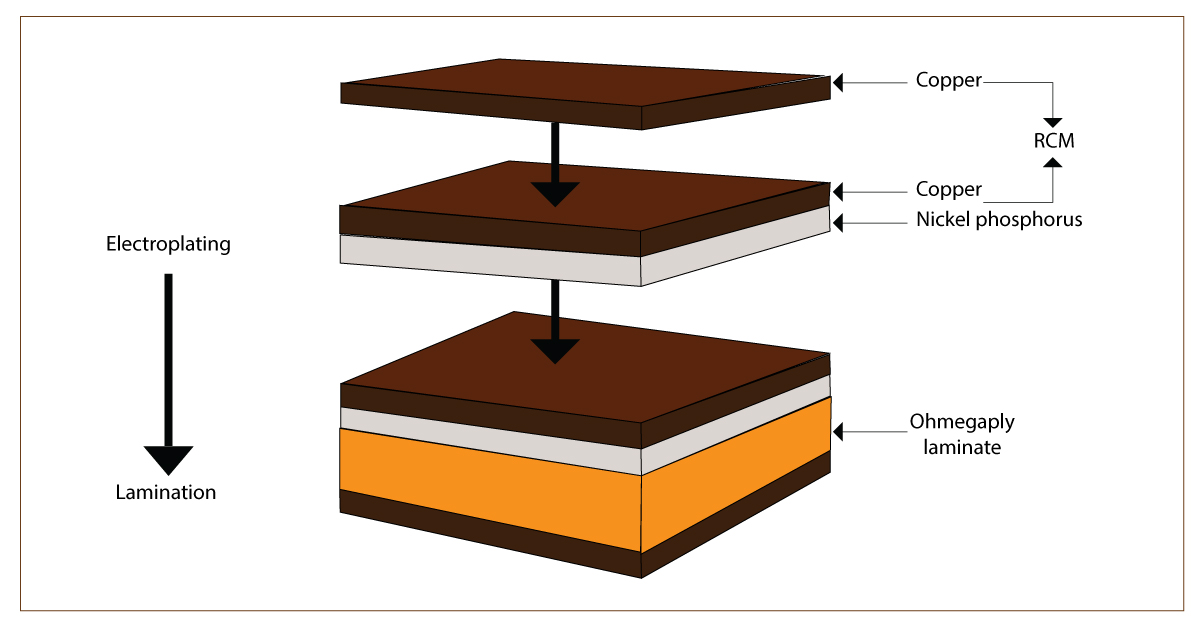
OhmegaPly embedded thin-film resistor material is a thin layer of nickel phosphorous metal alloy (NiP) electrodeposited on copper foil.
This is laminated to a dielectric material and subtractively processed to produce planar resistors. Due to its thin nature, it can be buried within layers without adding thickness or occupying space on the board like discrete resistors. Here, epoxies, polyimides, and PTFEs are all acceptable organic substrates.
Advantages of OhmegaPly
- Reduction of noise, crosstalk, and EMI
- Reduced series inductance and shorter signal paths
- Enhanced line impedance matching
- Better wiring due to the elimination of via
- Good reliability due to the elimination of solder joints
- Reduced form factors
- Improved active component density
- Better assembly yield
- Compatible with lead-free alloys
To learn how to select the right materials for your PCB designs, download our design guide.
PCB Material Design Guide
9 Chapters - 30 Pages - 40 Minute ReadWhat's Inside:
- Basic properties of the dielectric material to be considered
- Signal loss in PCB substrates
- Copper foil selection
- Key considerations for choosing PCB materials
Download Now
PCB layout for embedded passives
Layout designing is the first step in processing a circuit board. Setting up the design tool, creating the board outline, importing the netlist, placing components, routing, cleaning up silkscreen, processing DRC, and generating production documentation (Gerbers) constitute the PCB layout stage. Here, artwork layers focus on two printing stages:
- In the first printing stage, a composite image (negative) of resistors and conductors is printed and developed.

2. A defined image of resistor elements, which is typically used for the ground plane or voltage plane with most of the copper preserved, or a protected image of conductors, are used in signal planes.

Step-by-step fabrication process of OhmegaPly
OhmegaPly processing is a subtractive manufacturing process. CAD/CAM operators who switch between technologies must adjust artwork to compensate for dimensional stability and registration tolerances.
The fabrication process of OmegaPly begins with a laminate that has a thin resistance film under the copper. In the initial production film, the pad and trace layers are merged with the resistor body layer using Gerber, extended Gerber, or ODB++. Here is a picture of the pad/trace of a resistor.

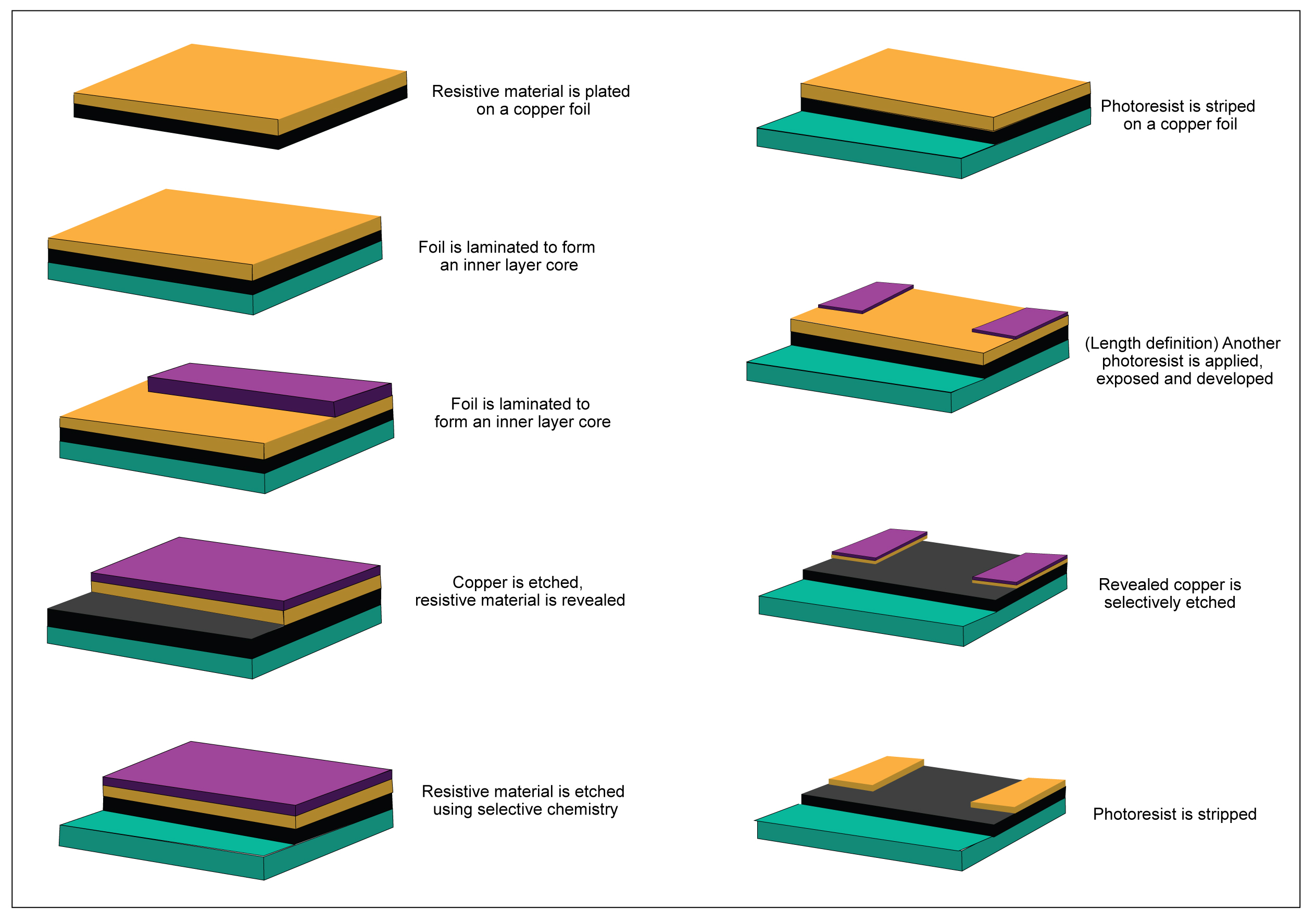
Given below is the list of sequential steps and their representations for processing OhmegaPly.
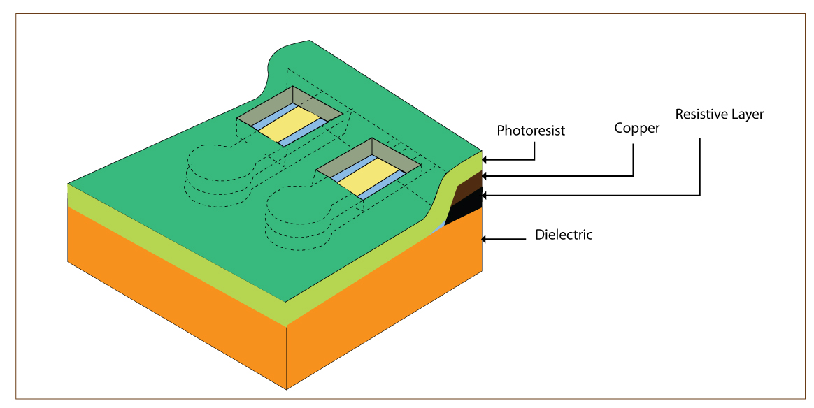
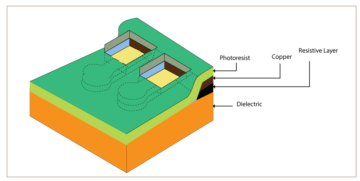
Application of photoresist
These steps are similar to multilayer board manufacturing. In this step, a photoresist (a layer of the photosensitive film) is applied to an OhmegaPly laminate material. It polymerizes upon exposure to UV light.
Printing and developing
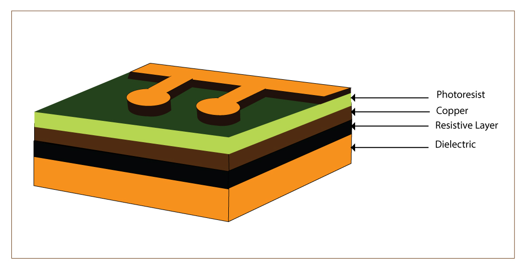
This step involves printing and developing a composite image. The panel will be placed under a computer-controlled laser. The computer scans the board’s surface and transforms it into a digital image. This digital image matches the specifications for the desired image in a pre-loaded CAD/CAM design file.
Copper etching
The next stage is to etch unwanted copper utilizing any conventional etchant. Unwanted copper is simply non-circuit copper. Removal of unwanted copper creates the desired circuit.
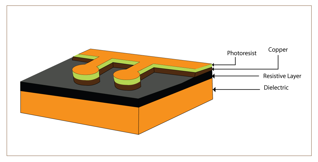
Resist etching
Copper etching is followed by resist etching. The unwanted resistive material is etched using copper sulfate (CuSO4) solution. This is commonly known as the second etch process.
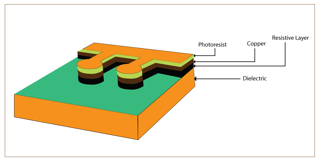
Photoresist stripping
During this process, the remaining photoresist is removed from the copper. The process involves dissolving caustic pellets (chemical agents) in water and then rinsing them with high-pressure water to break the photoresist.
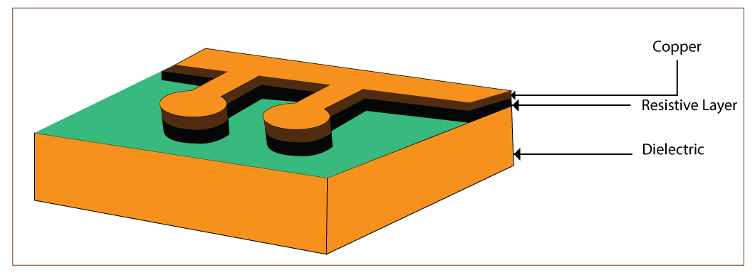
Photoresist application
In this step, the photoresist is applied again. This is followed by printing and developing the conductor-protect image. This is also called the second printing process.

Etching
Later, the excess copper is etched away from the designed resistor area using a selective alkaline etchant.
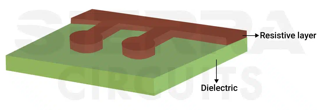
Photoresist stripping
This is the last stage, where the photoresist is stripped, and the desired pattern is created.
Sierra Circuits fabricates custom circuit boards within a quick turnaround time. See our rigid PCB manufacturing capabilities to learn more.
Design of elements: Best practices
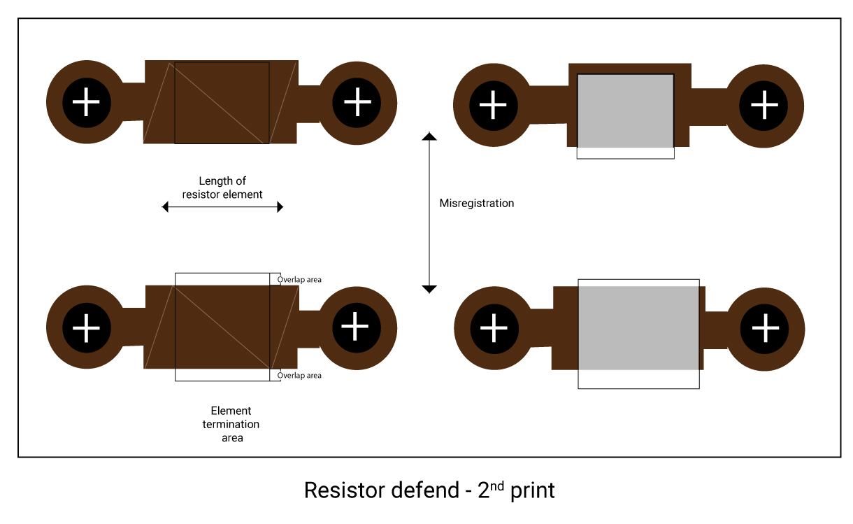
- Extend the length of the design element (5-10 mils) to compensate for any misregistration or misalignment of the artwork. The following image shows the composite’s design elements during the first print.
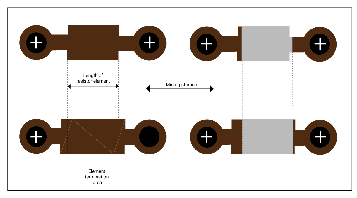
2. To balance any misregistration or misalignment of artwork in the image printing process, the overlap area should be 5 to 10 mils beyond the resistor’s width. The figure below gives an accurate representation of the overlap region.
Thermal isolation
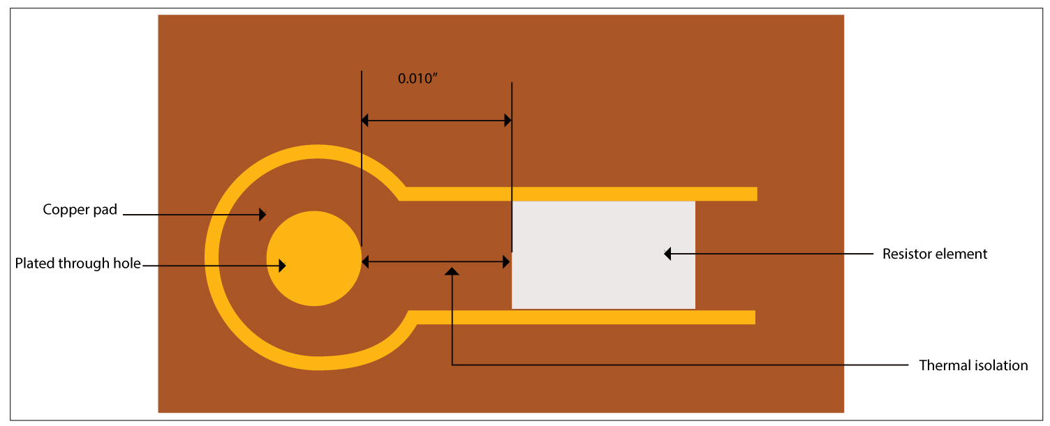
Thermal or mechanical isolation is intended to reduce the stress from the heat arising through a plated through via or surface mount pad during soldering or process reflow. Further, it serves as mechanical isolation, preventing resistance changes during drilling and/or dimensional movement of the board along the x, y, and z axes.
The recommended thermal isolation distance from the plated through hole to the resistor element is 10 mils, while laser drill microvias require a minimum distance of 5 mils.
Applications of OhmegaPly
OhmegaPly materials are used in:
- Interposer board
- Pull-up resistors in avionics
- Series termination resistors in BGA packages
- HDI PCBs
- Telecom switching cards
- OhmegaPly resistors in flex boards
- Buried resistor applications
TCR material
TCR® is an integrated thin-film resistor foil (grade 3 copper foil) that is available in different foil widths and thicknesses. The commonly available thickness values are 18 µm (0.5 oz) and 35 µm (1 oz).
TCR ® foil is available in three different resistivity alloys:
- Aluminum silicon, NCAS
- Chromium silicon monoxide, CrSiO
- Nickel chromium, NiCr
NiCr when used with TCR ® lowers fabrication steps by removing the conditions for a separate resistive layer etching.
Each of the three resistivity alloys can withstand multiple thermal excursions, like lead-free reflow, with minimal change to resistance and long-term stability.
The board processing method follows the same procedure as OhmegaPly. The only difference is TCR laminate material is used instead of OhmegaPly laminate.
Fabrication
- Circuit board fabrication with embedded passive technology (OhmegaPly and TCR) utilizes the same process as conventional manufacturing. In this process, embedded resistive materials are used as elements of the stack-up structure.
- Using NiCr resistor alloy decreases fabrication stages by eliminating the requirement of a separate resistive layer etch. It can be first etched in cupric chloride, followed by the ammoniacal etchant.
- Double-treated copper can also eliminate the requirement for laminate pre-cleaners and oxide treatments.
- To ensure properly defined resistor patterns, several key processes must be controlled and possibly modified.
- A few considerations include the equipment setup for the photoresist application, subsequent exposure, and development. Control over copper removal is also crucial for determining resistor length, which affects tolerances and resistance values.
Advantages of TCR
- Best PCB real estate utilization.
- Lead-free
- Easily recyclable
- Withstands multiple heat excursions
For decades, OhmegaPly and TCR have been the preferred embedded materials within critical military/aerospace applications.
Various modifications are in progress according to the different requirements. These materials will continue to play a key role in a variety of applications, including space exploration, telecommunication, cellular, medical, and industrial electronics.
If you have any questions related to OhmegaPly and TCR materials, please mention them in the comment section. Refer to our PCB material design guide, which explains the key considerations for choosing PCB materials


