Contents

On-demand webinar
How Good is My Shield? An Introduction to Transfer Impedance and Shielding Effectiveness
by Karen Burnham
Impedance matching is the way of configuring the input impedance of a load or the output impedance of its signal source. It is performed to achieve maximum power transfer and reduce the signal reflections from the load. In other words, for proper impedance control, the load impedance must be equal to the characteristic impedance of the transmission line. When the transmitted signal does not reflect it indicates that the load has absorbed all of it. Impedance matching in HDI is all about avoiding transmission faults, especially losses due to the resistance and PCB dielectric.
Microvias can be used to create production-friendly PCB traces for impedance-matched systems. BGA escape routing techniques and dogbone fanout structure can be used to implement impedance matching in HDI.

HDI PCB Design Guide
5 Chapters - 52 Pages - 60 Minute ReadWhat's Inside:
- Planning your stack-up and microvia structure
- Choosing the right materials
- Signal integrity and controlled impedance in HDI
- Manufacturing considerations for higher yields
Download Now
When do PCB traces need impedance matching?
Impedance matching is decided by the steepness and the rise/fall time of the signal rather than the frequency. If the rise/fall time (based on 10% to 90%) of the signal is shorter than six times the trace delay, then it’s called a high-speed signal. Here, precise impedance matching should be performed.
Challenges in HDI impedance matching
Designers come across the following challenges when implementing impedance matching in HDI:
- In high-density interconnect designs, small components have reduced pad-to-pad pitches such as BGAs. BGAs having pitches less than or equal to 0.65mm make routing traces and controlling their widths challenging. In such a case, via-in-pad and BGA escape routing techniques are used.
- Via in pads with blind vias is an advantage as they avoid via stubs, thus improving signal integrity.
- In an HDI board that requires impedance-controlled routing, carefully designed traces and stack-up are critical to ensure impedance is consistent with the signaling standard.
Also, read our post on the controlled impedance routing using Altium Designer.
Designing trace width for HDI impedance adjustments
The impedance of a trace is decided by its width and height from a reference plane. In HDI boards, where BGAs of fine pitch are used, careful selection of trace widths and height are employed to escape the traces between pads and vias in pads.
Impedance control with BGA escape routing in HDI PCBs
Several BGA components are used while dealing with high-density interconnect. To get traces in and out of the bottom of high-pin-count ball grid arrays, an escape routing scheme is required. In some circumstances, where controlled impedance is required such as with FPGAs and other high-speed components, BGA escape routing can be challenging.
The escape routing strategy to be utilized when designing a board is largely determined by the BGA pitch, which defines the permitted trace width to be put between solder balls. How thin the traces can be is also determined by the manufacturer’s limit, layer stack-up, and necessary impedance. When choosing an escape routing scheme, keep the following guidelines in mind.
- An escape routing technique for fine-pitch BGAs on moderate layer counts starts with a neck-down approach as a trace is routed into and out of the BGA.
- The outer traces can be routed straight onto the first row of solder pads on the board.
- The width of the trace for the second row of solder pads on a ball grid array is significantly decreased so that it may fit between the first row of pads.
- To get to the inner pads on the remaining rows, route through an inner layer. In general, route into two rows per signal layer while keeping impedance and HDI crosstalk in limit.
Controlled Impedance Design Guide
6 Chapters - 56 Pages - 60 Minute ReadWhat's Inside:
- Understanding why controlled impedance is necessary
- Stack-up design guidelines
- How to design for impedance
- Common mistakes to avoid
Download Now
Dogbone fanout
Dogbone fanout is the most popular BGA escape routing and fanout method (shown in the figure below). This fanout technique facilitates the placement of a via in a pad that is closer to the solder pad. Since the component is not soldered directly to the pad with the via, it does not require to be filled plated over. 1 mm BGAs and 0.8 mm BGAs are probably suitable for dogbone fanout.
Also, read how to breakout a .4mm BGA.
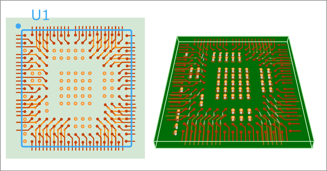
When the BGA pitch is smaller than 0.5 mm, microvia-in-pad escape routing technique is preferable. Instead of routing a small trace to the side of a pad, a microvia is placed directly into the solder pad. To prevent solder from wicking to the back of the board, the microvia is filled with conductive epoxy and plated with copper.
Microvias for BGA escape routing
If the pad size (including the annular ring) is small enough for a fine-pitch BGA then use microvias for inner layer BGA escape routing. The following characteristics differentiate a microvia from a conventional via:
- Via length: Vias should only traverse one or two layers at the most. A via can span more layers in case of standard thickness PCBs having very high layer counts, but this would need additional manufacturing procedures. Use stacked blind and buried vias that span a single layer wherever possible.
- Microvia aspect ratio: Microvia aspect ratios (depth divided by diameter) should be 0.75:1. Let us understand the same by considering an example of a 32-layer thickness board. As the layer thickness (for a 2-layer core) is two mils, the diameter should not be less than 2.7 mils.
Microvias can only be safely mechanically drilled down to 8 mils, however owing to frequent drill fractures, mechanical PCB drilling expenses per hole for 8 mils can approach the price of laser drilling. Mechanical vias have a lower throughput than laser-drilled vias because mechanical drilling must be done carefully to avoid bit fracture. As a result, once you start employing laser drilling, you’ll see a drop in total per-board costs.
To utilize a dogbone fanout on a 0.8 mm pitch BGA, the trace width must be 10 mils or less, and microvia must be even smaller (around 6 mils). In the case of finer-pitch ball grid arrays (0.5 mm), use filled and plated microvia-in-pad to route into the inner layers using 7 mil or 8 mil traces. This will give adequate spacing between the neighboring pads.
Microvias can be arranged as stacked or staggered to achieve the required routing density, regardless of the design style. Go through the IPC 6012 requirements to ensure that microvias and the surrounding annular rings are sized with optimum reliability. The relevance of microvia-in-pad in BGA escape routing can be understood by the fact that BGA pitch can reach as low as 0.3 mm in some instances.
How to place blind vias for escape routing
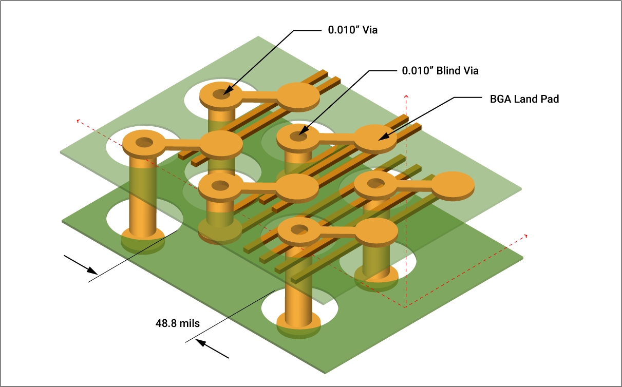
Blind vias are a valuable HDI design approach for freeing up additional inner-layer routing space. These type of vias double the routing space on the inner layers when used between through-hole vias. It allows for additional traces to link pins on the inner BGA rows. See the image given above; here, only two traces can escape between vias on the surface of this 1.0 mm BGA. However, six traces can now escape beneath the blind vias, and it increases the routing space by 30%.
Using this approach, one-fourth of the number of signal layers is required to connect a high-I/O BGA. Blind vias are placed in a cross, L-shaped, or diagonal pattern to form boulevards. The power and ground pin assignments determine which configuration to utilize.
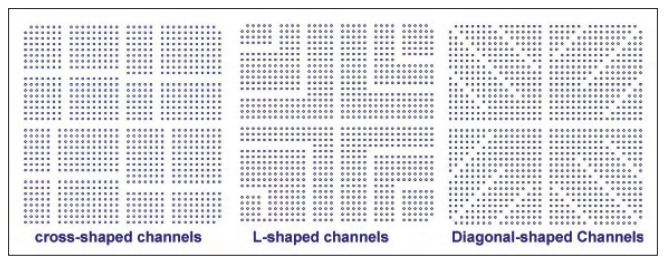
In his book, The HDI Handbook, Happy Holden gives an exaple of a 1153 pin (34 x 34), 1.0 mm BGA (shown in the below figure). Happy holden says,”There are 132 possible escape routes per signal layer (one trace between vias plus 20 traces in the cross-channel [five traces each]). This means that eight signal layers would be required (plus five reference planes) to connect this BGA to the rest of the circuit. The through-holes create a fence that makes breakout routing very layer-intensive.”
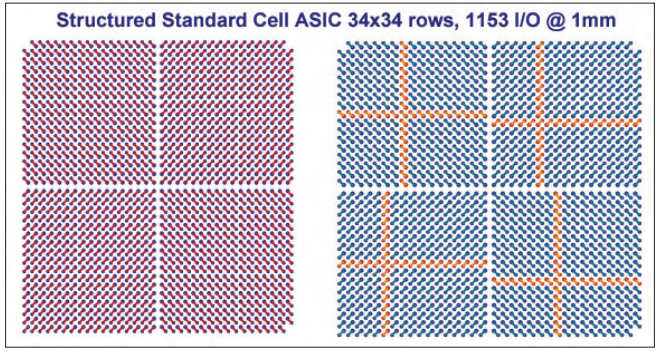
Happy Holden explains, “More traces per layer can be connected, and the overall number of signal layers can also be reduced by using boulevards to create additional routing space. Blind vias are utilized to create four cross-shaped boulevards (as shown in the figure). The newly-designed boulevards provide 48 more escapes per layer (8 x 6 traces), as well as improved signal integrity for the inner traces. It allows the removal of two routing layers and two reference planes.”
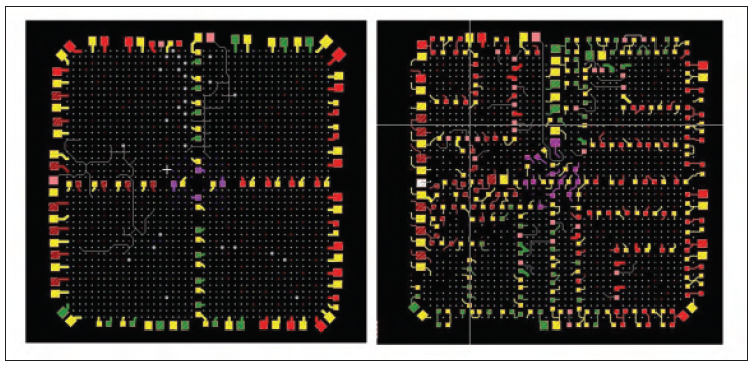
Further, he says, “On the secondary side of the circuit board, another advantage of creating boulevards with the blind via can be observed. The through-holes span through the whole board, but the boulevards now open within the BGA (shown in the figure). The figure on the left, shows 58 discretes linked by 104 vias under the BGA. On the right, the boulevards can link 183 discretes by sharing 366 vias.”
Fanout section length and trace width
Impedance is nearly always a factor when working with high-speed ICs. When examining the length of a fanout section, the relationship between fanout routing and impedance control comes into play. Because of the trace length (if exists) and parasitic capacitance/inductance of the via, the BGA fanout section will have its impedance.
First, check the signal bandwidth to determine if the signal will pick up on the trace’s impedance. The trace part of the BGA fanout can be disregarded if the trace length is significantly less than the wavelength corresponding to the high-end of the bandwidth. The best method is to compute the load impedance, which is a function of the fanout trace length, and the input impedance of the network created by the fanout traces (after neck-down).
Use a 10% restriction on the required length for the signal wavelength as a good approximation. A cautious 10% restriction for a digital signal with a knee frequency of 20GHz would result in a critical length of 0.73mm (stripline in an FR4 substrate). This means that bigger ICs, say FPGAs, will need an impedance-matched fanout for both single-ended and differential pairs.
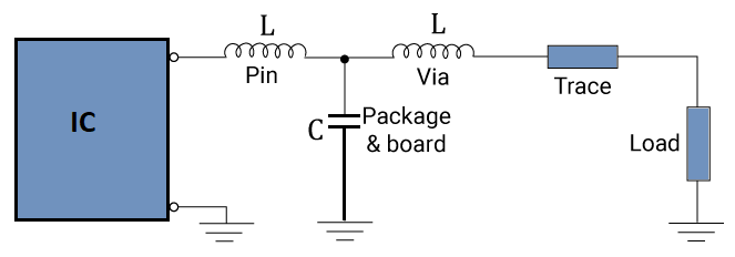
The via inductance, parasitic capacitance between the board and the land pad, and the pin inductance in the IC are crucial. A low pass T filter circuit is formed by combining these parts. The 3dB cutoff frequency will just be the typical number that can be evaluated from an LC tank circuit provided that the via inductance is set equal to the pin inductance. This T filter circuit works as an impedance matching circuit, modifying the driver IC’s output impedance.


Impedance matching of the fanout section is difficult without determining the via impedance linking the fanout trace to the internal trace. However, this fact can be ignored as long as the via section is short and directly spans only a few layers. The total input impedance that includes via and internal trace is dominated by the internal trace impedance while spanning through a small number of layers. This is why via impedance is not considered oftenly.
The main drawback is that high-speed BGA components, such as an FPGA, may require back drilling to remove the residual via stub beneath the BGA fanout. When working with HDI, blind, buried and laser-drilled microvias with very small diameters (less than 6 mils as per IPC) are used, which eliminates back drilling and limits via inductance only to the thickness of the layers spanned.
Since the layer thickness and distance to the reference plane of the trace will be reduced with higher layer counts, the trace width has to be decreased to compensate and keep the impedance at an appropriate value. If you are using differential pairs, think about trace coupling. To achieve impedance control, PCB design software with an integrated field solver can help in designing the right trace width for the HDI layer stack-up.
Read high-speed and HDI PCB design strategies by Syed Ubaid Ali Warsi to get expert advice on high-speed and HDI designs.
Why trace width cannot be more than the landing pad size?
- The width of a trace is proportional to its impedance and plays a crucial role when you enter the HDI regime. Vias will become so tiny that they must be manufactured as microvias once the trace width is small enough.
- If the impedance-controlled trace width is excessively wide, either reduce the PCB laminate thickness to shrink it or increase the landing pad size. From a reliability viewpoint, as long as the landing pad size surpasses the figure specified in the IPC standards, it will be fine.
- Create an impedance profile for PCB stack-up and use that width as a design guideline. Simply specify this value as a design rule after calculating the width required for impedance control. It’s preferable to perform a crosstalk simulation for the suggested trace width to see whether it would result in excessive crosstalk.
Impedance matching in HDI is related to maintaining signal quality since components and traces both are closely spaced. So, controlling impedance becomes a mind-boggling task. Efficient use of microvias is the key for impedance-matched HDI systems. Escape routing techniques for finer-pitch BGAs and the dogbone fanout method can be used to achieve impedance matching in HDI. To learn more about HDI circuit boards, read our design guide.
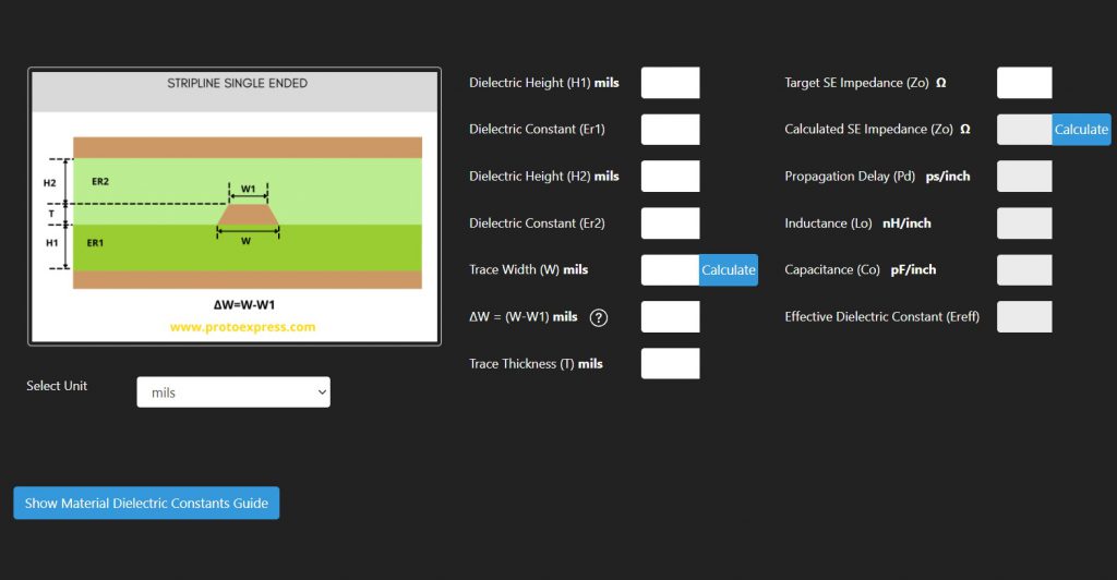
Try Sierra Circuits’ new Impedance Calculator
We have upgraded our Impedance Calculator, a free 3D field solder, which now uses the 2D numerical solution of Maxwell’s equations for PCB transmission lines. It renders accurate results suitable for use in circuit board manufacturing and engineering analysis. In addition to characteristic impedance of a transmission line, the tool also calculates line parameters such as capacitance, inductance, propagation delay per unit length, effective dielectric constant of the structure, and in the case of differential pairs, coupling coefficient, and even and odd mode characteristic parameters.


