Contents

On-demand webinar
How Good is My Shield? An Introduction to Transfer Impedance and Shielding Effectiveness
by Karen Burnham
A PCB consists of several parallel-spanning conductors separated by an insulator. These traces, along with dielectric material, form a capacitor, resulting in an unwanted parasitic capacitance or stray capacitance effect.
Parasitic elements in a PCB could be parasitic capacitance, parasitic resistance, and parasitic inductance. The parasitic capacitance effect is prominent in high-frequency boards when traces are closely placed. This effect is completely unwanted and affects the functionality of the device. It leads to problems like crosstalk, EMI, and signal integrity.
PCB designers dealing with high-frequency, high data rates, and mixed-signal boards must consider parasitic capacitance and inductance effects while designing the PCB layout.
What is parasitic capacitance in a PCB?
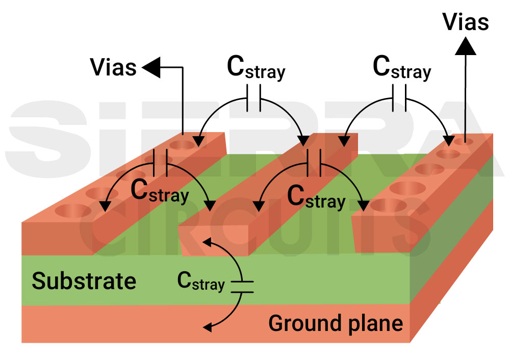
Parasitic capacitance or stray capacitance is the result of a virtual capacitor formed between two traces separated by a dielectric. It occurs due to the potential difference generated when the current-carrying traces run in close proximity. To learn more, read the role of trace current capacity in PCB design.
This effect is even possible if the conductors are appropriately insulated. It is not possible to avoid parasitic capacitance since no electrical circuit is ideal.
How is parasitic capacitance calculated?
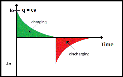
Parasitic capacitance is an inherent property of the conductors. It is the storage of per unit change in electric potential. The parasitic capacitance is calculated as C= q/v. Where C is the capacitance in farads, v is the voltage in volts, and q is the charge in coulombs.
- For a constant electrical signal that does not change over time, dv/dt = 0, which means no change in potential; hence i =0.
- If there is a capacitor in the circuit loop, dv/dt will converge to a fixed value, i.e., a change in potential, resulting in a current flow; hence i ≠ 0.
Trace capacitance calculation
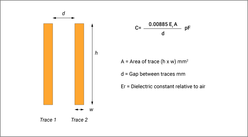
The capacitance of a parallel plate capacitor is given by C= (kA/11.3d)pF. Where C is capacitance, A is the plate area in cm2, k is the relative dielectric constant of board material, and d is the distance between the plates in cm.
What is parasitic capacitance effect?
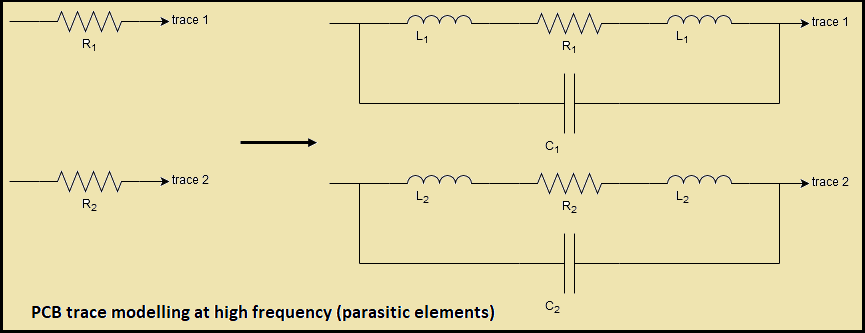
The parasitic capacitance effect is a matter of concern in high-frequency circuit boards. While operating at low frequencies, parasitic elements can be ignored since they do not really impact system functionality. Every pad in a circuit board has its parasitic capacitance, and every trace has parasitic inductance. Pads also add their parasitic resistance that stimulates IR losses. Parasitic capacitance can exist between conductors on PCBs, bare boards, PCBAs, assembled boards, and within component packages, especially surface mount devices (SMDs).
Since intrinsic capacitor plates have a potential difference, there is a chance of current flow. It does not matter whether the charges are stored between the capacitor plates; the current will not flow until there is a potential difference. As soon as this potential difference increases, a corresponding decrease in electron flow towards the load can be observed for the desired signal path, which negatively impacts signal integrity.

Signal Integrity eBook
6 Chapters - 53 Pages - 60 Minute ReadWhat's Inside:
- Impedance discontinuities
- Crosstalk
- Reflections, ringing, overshoot and undershoot
- Via stubs
Download Now
Difference between stray capacitance and parasitic capacitance?
The term stray capacitance is often used interchangeably with parasitic capacitance. However, parasitic capacitance accounts for the fact that it will hamper the circuit operation, while stray capacitance accounts for how unwanted capacitance is introduced.
What is stray capacitance?
Stray capacitance doesn’t always get induced due to the virtual capacitance formed between two PCB conductors, but also due to the effect of the surrounding environment. Hence, it is termed as stray capacitance.
What is parasitic resistance in a PCB?
Parasitic resistance exists in series along traces or as a shunt between the conductive elements.
What is parasitic inductance in a PCB?
Parasitic inductance exists along a trace and exhibits the behavior of storing and dissipating electrical energy, like an actual inductor. All conductors are inductive, and at high frequencies, the inductance of even relatively short pieces of wire or PCB traces may be important.
![]()
Where R is the wire radius, and L is the length.
How to find the inductance of a PCB trace?
Trace inductance increases with trace length and the lack of a ground plane.

Where W is the trace width, L is the trace length, and H is the trace thickness.
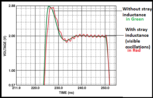
For example, a 2.54cm trace at the non-inverting input of a high-speed op-amp will result in 29nH stray inductance. And this is enough to initiate low-level oscillations. Stray inductance can be alleviated using a ground plane.
What causes parasitic capacitance?
At high frequencies, current flow in a circuit board is affected by parasitic capacitance. Since capacitors tend to become conductors when the frequency increases. Note that when frequency increases, the capacitor will act as a resistor of very small value (approaching a short circuit), resulting in excessive current flow.
Zc = 1/2πfC; therefore, as frequency increases, Zc decreases.
Parasitic capacitance can give you chills during high-frequency operation since a capacitor acts like a wire at an infinite frequency. This is why it can accidentally connect the reference plane of any PCB to the chassis.
Parasitic capacitance effects could be crosstalk and noise, undesirable feedback from the output, and the formation of resonant circuits. So, it is essential to give attention to the overall PCB design, specifically to the layout. A good layout should take utmost care while placing a conductive body by the side of another conductive body.
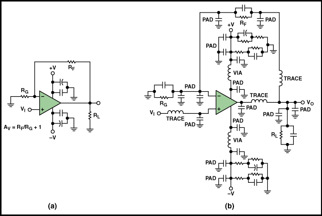
Parasitic elements include inductors formed by package leads, long traces, pad-to-ground, pad to power plane, and pad to trace capacitors, including interactions with vias, etc. Understand parasitic elements as parasites, a threat to your circuit performance. Unwanted and unavoidable, but controllable at the same time.
Let us take an example of a typical schematic of a non-inverting op-amp (figure a). Check figure b with parasitic elements:
To learn more about schematic symbols and schematic diagrams, read our article What’s the Meaning of a Schematic Diagram?
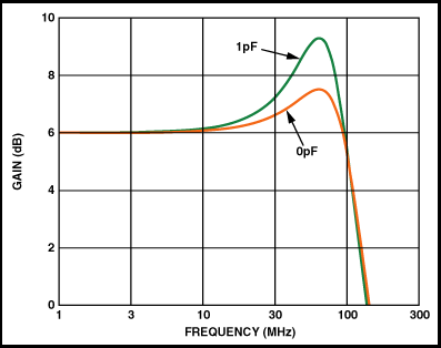
In high-speed circuits, a few tenths of a picofarad is enough to influence the circuit performance. For example, 1pF of parasitic capacitance at the inverting input can cause 2dB of peaking in the frequency domain. And if it is more than 1pF, it can cause instability and oscillations.
Vias also act as parasitic elements. They introduce both capacitance and inductance.
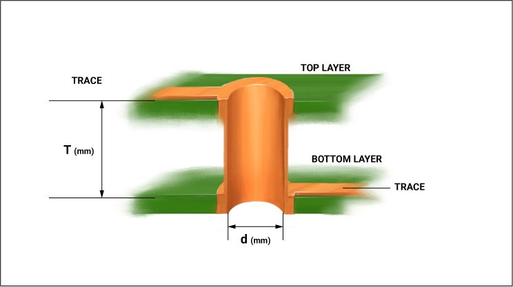
The parasitic inductance of a via is given by:

Where T is the thickness of the dielectric and d is the diameter of the via in cms.
The parasitic capacitance of a via is given by:

Where εr is the relative permeability of the board material, T is the thickness of the board, D1 is the diameter of the pad surrounding the via, and D2 is the diameter of the clearance hole in the ground plane. Read our post on how to choose PCB materials and laminates for fabrication.
Keep in mind that inductive vias combined with parasitic capacitance can form resonant circuits. The self-inductance of a via is small enough that these resonances are in the GHz range, but inductors added in series lower the resonant frequency. Do not put several vias on a critical trace of a high-speed circuit. Another concern is that the vias create holes in ground planes, creating ground loops. They should be avoided. The best analog layout must route all signal traces on the top layer of the PCB. Read 11 best high-speed PCB routing practices.

High-Speed PCB Design Guide
8 Chapters - 115 Pages - 150 Minute ReadWhat's Inside:
- Explanations of signal integrity issues
- Understanding transmission lines and controlled impedance
- Selection process of high-speed PCB materials
- High-speed layout guidelines
Download Now
Reducing parasitic capacitance in PCB layout
Capacitors block low-frequency and DC signals and pass high-frequency signals in electronic circuits. This property of capacitors to pass high-frequency signals (the rate at which capacitors discharge is another reason they are used in place of batteries, which are much slower) is responsible for stray capacitance problems in high-speed circuits.
For conductors, the stray capacitance can introduce EMI or noise that will propagate down the wires and cables or transfer to nearby adjacent traces. Usually, eliminating stray capacitance is not possible. Still, there are effective ways to mitigate it at the PCB layout level.
- Avoid parallel routing: With parallel routing, there is a maximum area between the two metals, so there is a maximum capacitance between them.
- Moating: Power planes are considered AC grounds and behave exactly the same as ground planes. So, removing the power planes is as important as removing the ground planes from the vicinity of a conductor. This technique is called moating.
- Use a Faraday shield or guard ring: A Faraday shield acts as a shielding plate, and it is placed between two traces to minimize the capacitive effects.
- Increase space between adjacent traces: Capacitance decreases with distance. Use the 2W or 3W rule.
- Avoid excessive usage of vias: Vias are necessary for connecting various layers of a PCB. But their excessive usage can increase the capacitance. To reduce PTH coupling, it is good to reduce annular rings around vias on layers where there is no connection. Thus, minimizing the number of vias from components, like BGAs.
- Careful component separation: Careful separation of components and wires, guard rings, power planes, ground planes, shielding between output and input, and proper termination of the transmission line is essential to reduce unwanted parasitic capacitance.
- Use low permittivity dielectric material: Keeping all other variables constant, the higher permittivity of a dielectric material produces greater stray capacitance, while a lower permittivity produces less stray capacitance.
- The signal layer should be sandwiched between two ground planes or between a ground plane and a power plane. In a 4-layer board, you can place the power plane on the bottom layer and route some sensitive traces between the power and ground planes. This will prevent EMI from signals in one layer from inducing noise in signals in another layer.
- Determine the right layer thickness: Thinner layers will decrease the loop area and the parasitic inductance, but they will increase the parasitic capacitance. You can use simulation tools with different layer stacks to determine the right layer thickness.
- Impedance matching: In high-speed digital applications, several data lines run at tens of Gbps, leading to impedance mismatch due to parasitic capacitance and inductance. Any mismatch caused by parasitics will produce reflections somewhere on the line, eventually increasing timing jitter and bit error rates. Impedance should be matched throughout the signal lines that carry high-speed data. For a detailed explanation, read how to limit impedance discontinuity and signal reflection in PCB transmission lines.
Measuring parasitic capacitance using TDR
What is the point of using a time-domain reflectometer (TDR) for measuring inductance or capacitance when there are several readily available, excellent-resolution LCR meters? The answer is TDR supports measurements on devices and structures as they exist in the circuit. While measuring parasitic elements, the surrounding environment of a device may affect the quantity to be measured. For valid measurements, it is critical to perform measurements on the device as it exists in the circuit.
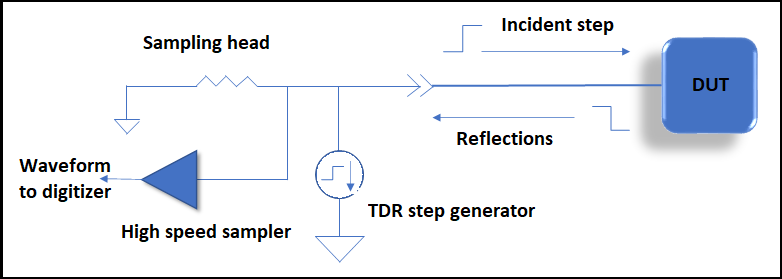
Additionally, when measuring the effects of devices or structures in systems that contain transmission lines, TDR allows separate measurements of transmission line characteristics and device characteristics without physically separating anything in the circuit. Allow us to explain how TDR measures quantities that are difficult to measure with an LCR meter.
Example: Let us take a PCB with a long, narrow trace over a ground plane, forming a microstrip line. At some point, the trace goes from the top of the PCB to the bottom through a via, and so on. Wherever the via passes through the ground plane, it has a small opening. Now, assume that the via adds capacitance to the ground.
Here, it would be a discrete capacitance to ground between the top and bottom transmission lines. We are assuming the transmission lines’ characteristics, and we need to measure the capacitance to ground between the two transmission lines.
For more on circuit simulation, see How Does Circuit Simulation Work?
An LCR meter measures the total capacitance between the trace-via-trace structure and ground. However, it is not possible to measure via capacitance and trace capacitance separately. For separate capacitance measurements, the traces are removed from the board. In this way, the capacitance between the via and ground can be measured. Obviously, this capacitance value cannot be considered correct for the model because traces are not included.
On the other hand, TDR fires a step wave on the PCB trace and observes the waveform reflected from via discontinuity. The amount of ‘excess’ capacitance caused by the via can be calculated by integrating and scaling the reflected waveform. This method provides the correct capacitance value for the model.
The mismatch between the two measurements exists because the LCR meter measured the total capacitance of the via while TDR measured the excess capacitance of the via. If the series inductance of the via was zero, then its total capacitance would be considered the same as its excess capacitance.
Since the series inductance of the via is not zero, a complete model of the via must be considered, including both its series inductance and its shunt capacitance. Considering that the via is capacitive, now the model can be simplified by eliminating the series inductance and including only the excess capacitance in place of the total capacitance.
The excess capacitance measured using TDR is the correct value for the model. The trace-via-trace structure is modeled first to predict the effect of the via on the signals propagating along the traces. TDR propagates an input pulse along the trace to make the measurement. In this way, TDR provides a direct measurement of the unknown quantity.
Unfortunately, it is not possible to completely eliminate parasitic elements. However, there are some simple PCB layout choices you can make to reduce the parasitic capacitance effects. Selecting the right components can also prevent signal problems that arise from parasitic capacitance and inductance. Accurate design and manufacturing decisions can control these parasitics.


