


Contents

On-demand webinar
How Good is My Shield? An Introduction to Transfer Impedance and Shielding Effectiveness
by Karen Burnham
Getting your first PCB manufactured can be quite simple if you just know the steps involved.
In this article, you’ll learn how to get your prototype manufactured in 6 simple steps—from designing your circuit board to placing the final order.
Whether you’re a beginner or an experienced PCB designer, these steps will help you build an efficient prototype.
Watch the full webinar here: Everything you need to know to get your first PCB manufactured
Highlights:
To get your PCB manufactured:
- Evaluate potential fabricators based on cost, quality, and turnaround time to ensure they meet your project’s specific needs.
- Check if your design adheres to the manufacturer’s capabilities (trace width, drill size, and stack-up feasibility). Run a DRC before submission.
- Include all necessary files, such as Gerber files/IPC-2581/ODB++, BOM, netlist, and assembly drawings. Clearly specify fabrication notes and special instructions.
- Engage with the CM’s engineering team to optimize your design for manufacturability and address any potential issues.
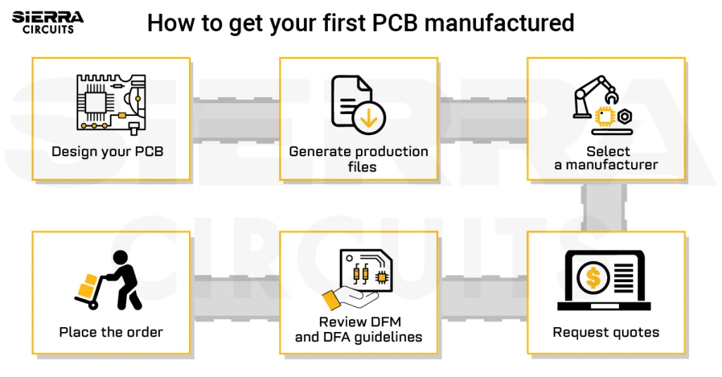
6 steps to get your first PCB manufactured
Here are the key steps involved in PCB prototyping for beginners:
Step-1: Design your circuit board: Utilize EDA tools to create detailed PCB schematics and layouts.
Step-2: Generate production files: Export the necessary PCB manufacturing files, such as Gerber files/IPC-2581/ODB++.
Step-3: Select a manufacturer: Evaluate potential manufacturers based on cost, quality, capabilities, and certifications.
Step-4: Request quotes: Obtain pricing and lead times from multiple manufacturers to make an informed decision.
Step-5: Review DFM and DFA guidelines: Ensure your design complies with DFM and DFA standards to prevent potential issues during production.
Step-6: Place your first PCB order: Finalize specifications and submit your updated design files.
Download our eBook to learn how to design for manufacturing.

Design for Manufacturing Handbook
10 Chapters - 40 Pages - 45 Minute ReadWhat's Inside:
- Annular rings: avoid drill breakouts
- Vias: optimize your design
- Trace width and space: follow the best practices
- Solder mask and silkscreen: get the must-knows
Download Now
How to evaluate and choose a PCB manufacturer
Your CM should have the expertise to handle your specific PCB type—whether high-speed, RF and microwave, HDI, or rigid-flex.
This section outlines 4 key factors to evaluate a PCB manufacturer, with essential queries to understand their capabilities.

1. Manufacturing expertise
Assess the manufacturer’s ability to produce the type of PCB you need.
For instance, if you’re designing an HDI board, evaluate the CM’s expertise in laser drilling, microvias, blind and buried vias, and precise impedance control. Additionally, check if they use advanced equipment for sequential lamination and fine-line etching, which are critical for HDI fabrication.
Check if they offer design for manufacturability (DFM) analysis to identify potential production issues early on.
Ask these 5 questions to your CM to understand their capabilities better:

2. Quality assurance and certifications
To ensure high-quality boards, ensure your manufacturer has the following:
- Certifications like ISO 9001 (quality), AS-9100D (aerospace), and ITAR (military).
- Experience with complex designs (hybrid stack-ups, fine-pitch BGAs, multi-lamination).
- Tight tolerance and precision in trace width, hole size, copper thickness, and materials (FR4, Rogers, PTFE)
3. Turnaround time
Make sure the fab house can deliver your boards on time. Delays can lead to increased costs and project setbacks.
Some manufacturers offer standard turnaround times of 5 to 6 days, while others can provide quickturn boards within 1 to 3 days. Understanding their lead time capabilities helps you meet the deadlines.
4. Cost structure
Set a budget based on design complexity and production volume. Low prices can be tempting; however, cutting costs too much can lead to defects, delays, and higher long-term expenses.
Get quotes from multiple manufacturers, considering tooling, testing, and any special requirement costs. Comparing quotes from more fabricators helps you understand pricing structures.
How to evaluate a PCB manufacturer’s capabilities
Before placing an order, one thing to keep in mind is your manufacturer must match the capabilities that your design demands.
Here are the critical factors to assess:
1. Trace width and spacing limits
The minimum trace width and spacing determine how dense signals can be routed on the board.
Manufacturers typically support trace widths between 2 and 4 mil, which is crucial for high-density PCB designs.

To learn more, check out our rigid PCB manufacturing services.
2. Annular ring specifications
The annular ring is the copper pad surrounding a drilled hole (via). If it’s too small, there is a risk of breakout or weak connections.
Look for manufacturers that support at least 2 mil for laser-drilled vias and 3–5 mil for mechanically drilled holes to ensure strong electrical and mechanical reliability.
3. Layer count and board thickness options
Standard PCB stack-ups typically include 2, 4, or 6 layers, while advanced designs can exceed 30 layers.
Board thickness plays a crucial role in mechanical strength and thermal dissipation. A reliable manufacturer should provide thickness options from 5 to 10 mil to meet diverse design and performance requirements.
4. Maximum lamination cycles
Lamination cycles bond PCB layers together. Excessive cycles can cause delamination or warping. Ensure your manufacturer can handle the necessary cycles while maintaining material integrity, especially for HDI, rigid-flex, or multilayer PCBs. Generally, it is not recommended to have more than 3 lam cycles.
5. PCB material options
PCB material selection directly impacts thermal performance, signal integrity, and mechanical strength.
Different applications require different materials, such as FR4 for general-purpose use, Rogers for RF applications, or PTFE for high-frequency circuits.
If your design requires a material the manufacturer doesn’t support, you may face delays or compromises in performance.
6. Advanced manufacturing capabilities
Check if the CM offers advanced capabilities for specialized boards like RF, micro, HDI, or rigid-flex, as they require advanced manufacturing techniques, such as tightly controlled impedance tolerance, etching, laser drilling, or sequential lamination.
7. Material movement and scaling prediction
During lamination, PCB materials can shrink, expand, or warp due to heat and pressure. Manufacturers should have methods to predict scaling and material movement to prevent misalignment issues.
At Sierra Circuits, we use Pluritec machines to inspect material shifts during the manufacturing process, ensuring dimensional stability.
8. Testing and quality assurance
Rigorous testing ensures the reliability and quality of the final PCB. Confirm whether the manufacturer offers the following testing options:
- Automated optical inspection (AOI): Detects surface defects like opens, shorts, and misaligned components.
- X-ray inspection: Identifies internal defects such as voids in vias and solder joints.
- Flying probe testing (FPT): Evaluates electrical connectivity without requiring custom test fixtures.
By thoroughly analyzing a manufacturer’s capabilities, you can ensure they meet your specific design needs and deliver a high-quality PCB.
What does your PCB fabricator expect from you?
Before submitting your design files to your CM, ensure your design is optimized for manufacturability. Manufacturers have specific capabilities and requirements, and failing to adhere to them can lead to fabrication errors, delays, or increased costs.

Here’s what your manufacturer expects from you:
- Design as per fabricator’s capabilities:
- Ensure the design adheres to the manufacturer’s capabilities, such as minimum trace width/spacing, drill size, stack-up feasibility, solder mask, and surface finish compatibility.
- Manufacturers have limitations based on their equipment, processes, and expertise. When designing your PCB prototype, always refer to the manufacturer’s capabilities document or spec sheet.
- Adherence to clearance requirements:
- Confirm trace, pad, via, and board edge clearances with your CM to avoid fab errors. Insufficient clearances can lead to short circuits, etching issues, or mechanical failures.
- Design rule check (DRC):
- Run a DRC before submitting the design files. It ensures your design adheres to the predefined (compatible with the manufacturer’s capability) design rules.
- PCB BOM file:
- Compile a detailed list of all the components, including part numbers (MPNs), quantities, reference designators, and footprints.
- Upload the BOM to the manufacturer’s portal and save it to your project.
- If needed, request assistance from the engineering support team to review datasheets, suggest alternative MPNs, or source hard-to-find parts.
- Comprehensive stack-up details:
- Clearly mention the layer count, names (signal/power/ground), material preferences, controlled impedance requirements, and target thickness in the stack-up document.
- Controlled impedance specifications (if required):
- Specify target values (e.g., 50Ω single-ended, 100Ω differential) and tolerance (±10%) and include them in your documentation. If needed, request assistance from the CM to verify impedance values or impedance calculations.
- Correct PCB file format:
- Provide the updated design files in the correct PCB file format (Gerber, ODB++, or IPC-2581). Include netlist, BOM files, and pick-and-place files.
- Detailed fab and assembly notes:
- Include fabrication notes, drill data, assembly drawings, and special instructions along with your production files. Use a standardized template to ensure consistency and clarity.
Checklist to submit your design files
Ensure your design files are complete and correctly formatted for a smooth PCB manufacturing process. Verify the following before submission:
- Include all the required layers (top and bottom copper, solder mask, silkscreen, etc.). Ensure files are in a standard format and include a layer map or readme file to clarify which file corresponds to each layer.
- Provide a clear stack-up diagram, including material thickness, copper weights, and dielectric layers. For multilayer boards, include prepreg and core layers.
- Specify plated vs. non-plated holes, finished hole sizes, and tolerances in your NC drill files.
- Submit a complete BOM listing part numbers, package types, alternative MPNs, and vendor details.

A sample of a BOM with MPNs, required part quantities, reference designators, and description. 
- Provide centroid files (pick-and-place files) for SMT assembly, detailing exact part locations, orientations, and reference designators.
- Define panelization requirements, including tab routing, V-scoring, and fiducial marks for assembly alignment.
- Indicate any mechanical constraints such as mating connectors, heat sinks, mounting holes, and keep-out zones for critical areas.
- Include special instructions, such as via tenting, castellated holes, controlled depth routing, and edge plating.
- Deliver IPC netlist files for electrical testing to verify connectivity and detect shorts or opens.
- Provide a board outline file (e.g., Gerber or DXF) defining the physical dimensions, cutouts, and any edge features like chamfers or slots.

Gerber files with aperture and layer information.

14 must-have details in your PCB fabrication notes
PCB fabrication notes communicate essential specifications that guide the manufacturing process, ensuring that the circuit design is built accurately. Include the following details clearly in the fabrication drawing:
- Specify the applicable IPC class (class 2, class 3, or class 3/A).
- Mention the board material (e.g., Rogers 4350B, I-TeraMT40, FR4) based on electrical, thermal, and mechanical requirements.
- Define copper thickness for each layer (e.g., 1 oz, 2 oz) and state the final copper thickness after plating.
- Detail the complete stack-up, including signal, power, and ground planes, along with core and prepreg thicknesses.
- Indicate trace width, spacing, and reference layers for controlled impedance traces. Specify target impedance (e.g., 50 Ω, 100 Ω differential) and tolerances (e.g., ±10%).
- Describe via types (e.g., through-hole, blind, buried) with precise sizes, and clarify whether they need to be filled (e.g., conductive epoxy, non-conductive), plated, tented, or plugged.
- State outgassing requirements if the PCB is intended for vacuum or space applications.
- Define the solder mask color, type, and clearance requirements to prevent unintentional solder bridging.
- Specify the silkscreen color, font, dimensions, and any restrictions on placement for readability and clarity.
- Choose the type of surface finish (e.g., ENIG, HASL, OSP) based on assembly and longevity needs.
- Set manufacturing tolerances for board dimensions, hole sizes, bow and twist limits, and clearance allowances.
- Mandate electrical testing requirements, including flying probe or bed-of-nails testing, impedance validation, and high-voltage isolation tests if needed.
- Include any special requirements such as date codes, UL markings, serialization, edge plating, counterbores, controlled depth drilling, or conformal coating needs.
- Mark fiducial locations and sizes for SMT assembly alignment if applicable.
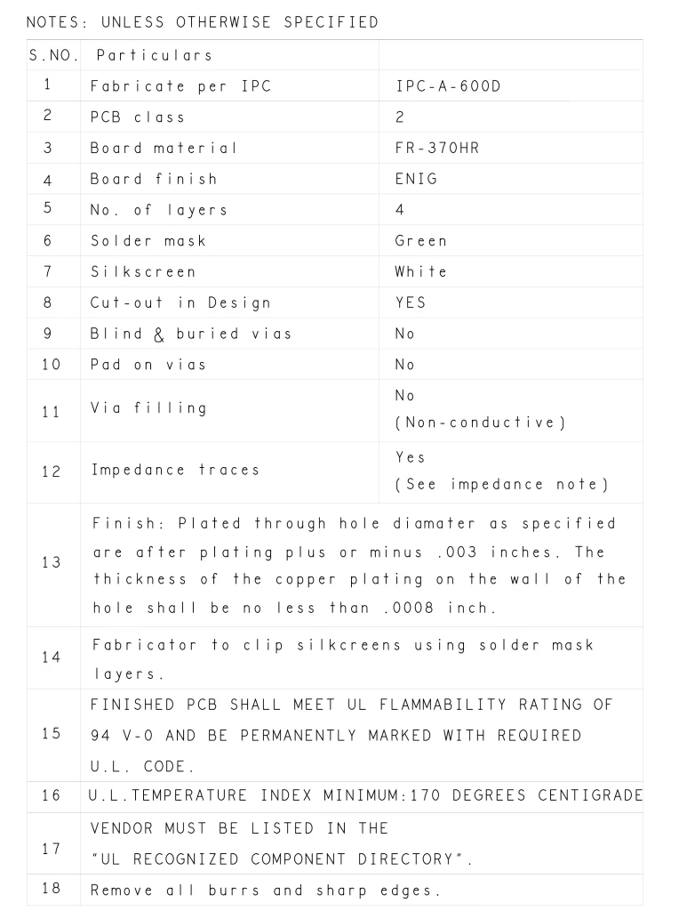
An example of standard fab notes.

14 essential details to cover in your PCB assembly notes
Assembly drawings provide clear instructions for component placement, soldering, and inspection.
Here’s what you need to do for a perfect assembly drawing:
- Label component reference designators (e.g., R1, C3) and polarity indicators (e.g., cathode/anode markings) for all parts and ensure they match the BOM and PCB silkscreen to prevent assembly errors.
- Mark global fiducials and provide local fiducial markers near fine-pitch or BGA components for precise alignment during automated assembly.
- Include fiducial locations and dimensions to aid pick-and-place accuracy.
- Specify pin 1 marking locations for ICs, connectors, and other polarized components using silkscreen dots, triangles, or annotations. Clarify any rotation requirements to prevent misplacement during assembly.

- Define solder specifications, including the type of solder (e.g., lead-free or leaded), solder thickness, reflow profiles, and any special requirements for soldering sensitive components.
- Indicate the application areas for solder mask and paste mask layers, especially for fine-pitch and BGA components, to prevent solder bridging or insufficient solder deposition.
- List conformal coating specifications, such as type, thickness, and coverage requirements, to protect against environmental factors like moisture and dust.
- State wash or no wash requirements for each component, especially for sensitive parts like MEMS or unsealed relays.
- Include instructions for post-assembly automated X-ray inspection (AXI) and automated optical inspection (AOI), with details on component types requiring special attention, such as BGAs, QFNs, or other leadless packages.
- Note height restrictions and mechanical constraints for components (e.g., max height near edge) to ensure fit within enclosures or assemblies.
- Show mounting hole locations, cutouts, and mechanical features like slots or edge connectors.
- Highlight unique handling needs for critical components, such as ESD-sensitive devices, heatsinks, or connectors.
- Designate test point locations for in-circuit testing (ICT) or functional testing, labeled with net names or purposes.
- Outline keep-out zones where no components or solder should be placed (e.g., under RF shields or near mounting screws).
Download our design guide for DFA tips.

Design for Assembly Handbook
6 Chapters - 50 Pages - 70 Minute ReadWhat's Inside:
- Recommended layout for components
- Common PCB assembly defects
- Factors that impact the cost of the PCB assembly, including:
- Component packages
- Board assembly volumes
Download Now
8 common PCB errors caused by DFM ignorance
By following circuit board DFM rules, you can identify potential manufacturing flaws in the design phase. If ignored, you may encounter the following defects:
- Etching issues: Inaccurate etching can remove excess material, causing inconsistent trace widths, unintended shorts, or broken circuits. Conversely, under-etching may reduce trace current capacity, affecting signal integrity.
- Solder mask misalignment: Improper alignment can expose unintended areas, leading to shorts or corrosion. Excessive clearance reduces electrical insulation, increasing solder bridge risks.
- Stack-up imbalance: Unbalanced stack-ups and improper copper distribution can cause PCB warping, hindering correct assembly.
- Insufficient solder mask clearance: Inaccurate or missing solder paste can result in solder voids, compromising joint strength and component reliability.
- Inaccurate thermal relief: This can create voids between thermal areas and pads, leading to poor solder connections due to insufficient heat transfer.
- Drill misalignment: Misaligned drilling during CNC processes can shift plated-through holes, causing annular ring issues like tangency and breakouts.
- Unfilled vias: Vias without proper filling can allow the solder to wick away during reflow, resulting in weak or missing solder joints.
- Copper slivers: Narrow gaps between copper features can leave small floating wedges after etching, risking shorts or reliability failures.
For practical design tips to avoid these errors, read 5 DFM issues designers should check before PCB manufacturing.
While DFM ensures manufacturability, the PCB design for assembly guarantees efficient component placement, soldering, and testing.
Sierra Circuits’ 6-step process for effective DFM analysis

Step-1: Import the design files into the CAM tool
-
- This step involves importing the design files (Gerber, ODB++, IPC-2581, etc.), drill files, netlist, and other design data.
- The CAM software then translates this data and extracts critical data such as layer stack-up, drill sizes, trace widths, and spacing.
Step-2: Review key design elements
-
- Once the files are imported, a detailed review of several critical aspects of your design ia carried out to check for common manufacturability issues
- The netlist (from the schematic) is compared against the PCB layout to detect shorts or open circuits.
- Measure annular rings (the copper pad surrounding a drilled hole) to ensure they meet minimum requirements. Flag undersized rings, which risk drill breakout or tangency during assembly.
- Checks for clearance between copper features (traces, pads, vias) and other features and the board edges to prevent mechanical damage during routing or depanelization.
- The solder mask is reviewed to ensure proper coverage and alignment with pads and traces.
- The silkscreen is checked for legibility and placement, ensuring that component labels and markings do not overlap with pads or vias.
Step-3: Compile the DFM report
-
- After reviewing the design, a detailed list of all manufacturability concerns and screenshots with annotations (e.g., circles around problematic traces) categorized by severity (e.g., critical, moderate, minor) is compiled.
- This report provides a clear overview of the issues that need to be addressed.
Step-4: For every issue identified, the DFM report includes actionable recommendations on how to adjust the design.
Step-5: Include screenshots and visually highlight areas of concern in the report.
Step-6: Final approval for production
-
- Once all DFM concerns have been addressed and the design has been revised to meet all manufacturability requirements. The project moves into the production phase, where the PCB is fabricated and assembled according to the approved specifications.
Use Sierra Circuits’ Better DFM tool to ensure your PCB’s manufacturability. It offers a detailed DFM report along with an instant price quote.
How to get a quote and order PCBs from Sierra Circuits
Below is a step-by-step guide to ensure a smooth quoting and ordering process at Sierra Circuits.

Step-1: Start a custom quote and upload design files
-
- Go to Sierra Circuits’ homepage and click on Quote Now. Select your PCB type and enter the specs. This includes board dimensions, layer count, copper weight, material type (e.g., FR4, Rogers), surface finish (e.g., ENIG, HASL), solder mask, and silkscreen.
- Select ITAR compliance or mil-spec standards if applicable to your project.
- Upload Gerber, ODB++, or IPC-2581 files along with the BOM and pick-and-place (centroid) files for assembly.
Step-2: Technical review
-
- Our engineering team will review your design to check for missing files and discrepancies.
- If there are any issues, our experts will get in touch with you (through the customer portal and emails) and resolve them.
Step-3: Receive a tailored quote
-
- You will get a pricing estimate based on board complexity, materials, stack-up, order quantity, and turnaround time.
Step-4: Order approval
-
- Once you approve the quote and place the order, our sales team will assign an SPx tracking number to your project.
- Use the SPx number in our customer portal to monitor real-time order status and communicate with our team.
Step-5: DFM and DFA analyses
-
- Our DFM and DFA experts will thoroughly inspect your design.
- Checks include trace-to-trace spacing, annular ring violations, solder mask clearances, drill alignment, and stack-up feasibility.
- If any issues arise, you’ll receive an IST. Resolve these issue tickets to prevent production delays.
Step-6: Manufacturing and delivery
-
- Once all design concerns are resolved, production begins.
- If modifications are required after placing an order, submit an engineering change order (ECO) immediately.
- File a customer support ticket (CST) for any post-shipment concerns.
- Your PCBs will be shipped on time, directly to your doorstep.
Key takeaways:
- Understand your CM’s capability before finalizing the board specs.
- Provide detailed documentation, including impedance requirements, stack-up, assembly instructions, and fab notes.
- Ensure your fabricator offers testing options like AOI, X-ray, and flying probe to verify electrical connectivity and detect errors.
- Compare quotes from various fabricators. Do not compromise on materials and manufacturing precision.
- Monitor order status through the manufacturer’s portal, respond quickly to engineering queries, and submit change orders if modifications are needed post-submission.
When you’re selecting a prototype fabricator, consider their manufacturing expertise, verify the quality assurance and certifications, understand the pricing structure, and ensure they can meet your project deadlines.
Have any design queries? Post them on our forum, SierraConnect. Our PCB experts will answer them.


Start the discussion at sierraconnect.protoexpress.com