Contents

On-demand webinar
How Good is My Shield? An Introduction to Transfer Impedance and Shielding Effectiveness
by Karen Burnham
Designing mixed-signal PCBs presents unique challenges in managing the interactions between digital and analog signals. Digital circuits generate noise due to switching operations, which can interfere with sensitive analog components.
By isolating the analog and digital components, implementing the right signal protocols, and providing short return paths you ensure a reliable mixed-signal board.
In this article, you’ll learn the steps for designing mixed-signal PCBs while addressing the common challenges you might face.
Highlights:
- Segregate digital and analog components such as microcontrollers, FPGAs, OPAMs, filters, and sensors.
- Select components with appropriate signal interfaces.
- Place ground planes efficiently to minimize interference.
- Distribute stable power for the analog and digital circuits.
What is mixed-signal design?
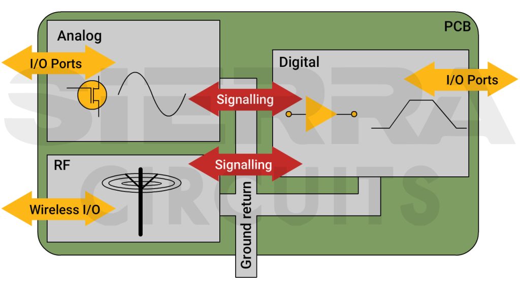
A mixed-signal layout includes both analog and digital circuits. Analog circuits work with continuous signals like audio or sensor outputs, while digital circuits process discrete values, often representing binary data.
They are commonly found in applications such as telecommunications, data acquisition systems, audio devices, and control systems. Both high-speed digital and sensitive analog components must function harmoniously to maintain signal integrity.
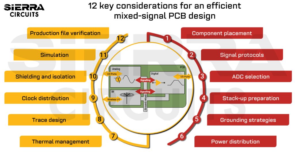
12 steps to design an efficient mixed-signal PCB
Taking precautions during stack-up design, component placement, and routing can help you design high-performing circuits without any errors. Here’s the step-by-step procedure for creating noise-resistant mixed-signal PCBs.
Step 1: Segregate different sections in mixed-signal PCB design
1.1 Identify analog and digital sections
When designing a floor plan, follow the signal path outlined in the PCB schematic. Identify critical functional blocks, signals, and their interconnections.
Typically, analog sections will have components like operational amplifiers, filters, voltage references, and sensors. If a system includes a single mixed-signal ADC or DAC with low digital currents, you can treat it as an analog component.
The digital section includes components like microcontrollers, FPGAs, and memory chips, which handle binary data. Isolating these parts helps reduce noise coupling between high-speed digital and sensitive analog signals.
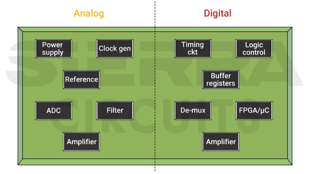
You can also reduce the noise by selecting appropriate electronic components for the application. For instance, choose op-amps with a high common mode rejection ratio (CMRR) for better noise immunity.
To learn how to build an efficient circuit, see 8 best electronic circuit design practices.
1.2 Strategically place analog and digital circuits to reduce interference
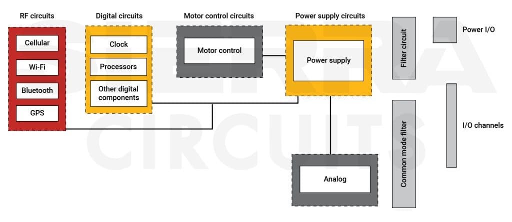
Analog circuits are highly noise-sensitive, while digital circuits operate with high-speed signals that can induce EM fields. If you place these two systems close, they can interfere with each other, degrading performance and reliability.
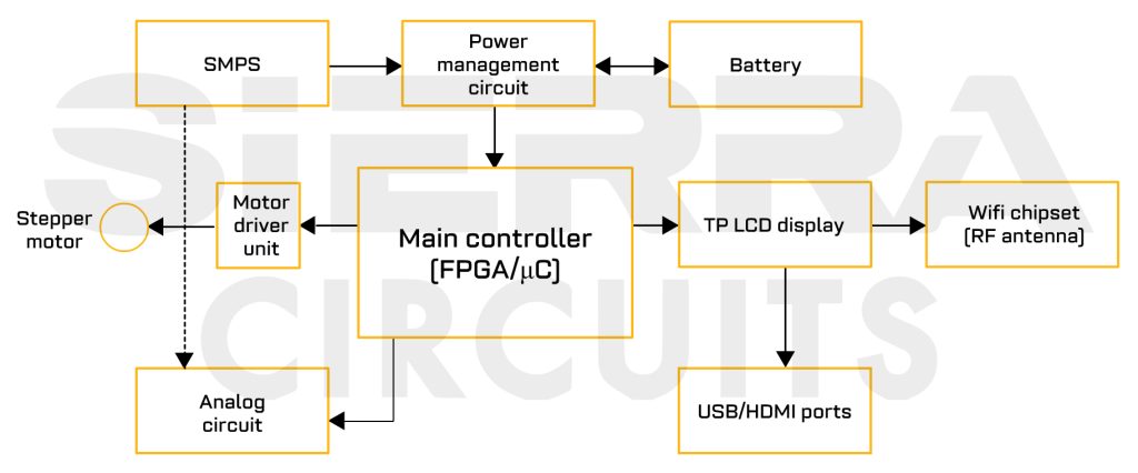
Consider a simple example of a control system configuring motors using analog sensors. Here, we have connected the central control unit (microcontroller) to a motor through driver circuits. We have powered the PCB using a switch-mode power supply (SMPS), a power management unit, and a battery circuit.
In the analog section, we have sensors that detect pressure, temperature, motor direction, and speed. There are USB/HDMI port connectors for external connection and a TP LCD. There is also an RF circuitry for Wi-Fi connectivity. We have separated the analog section from digital and RF circuits.
Additionally, the antenna in the RF section operates at high frequencies and is prone to noise. Hence, you should place them away from noise sources like power circuits and stepper motors.
For antenna placement tips, see antenna integration and RF design guidelines for 5G PCBs.
Step 2: Select components with appropriate interfaces
In mixed-signal PCB designs, you must consider the unique demands of different signal types and frequencies. Here’s a quick infographic on different signal protocols.
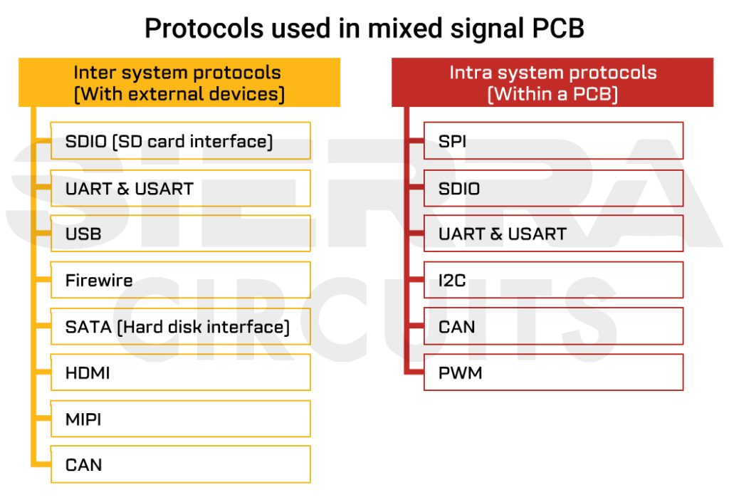
Managing them efficiently will ensure that digital and analog signals can be processed appropriately. The choice of signal protocol depends on factors like speed, complexity, and the application’s specific requirements. Here’s a brief overview of different protocols:
2.1 Serial peripheral interface (SPI)
It is a synchronous serial communication protocol that allows multiple devices to communicate with a master device. This uses four wires for data transfer:
- Master out slave in (MOSI)
- Master in slave out (MISO)
- Serial clock (SCK)
- Slave Select (SS)
SPI supports higher data rates and is suitable for short-distance communication. High-speed PCB designers commonly use this for connecting sensors, memory devices, and displays. For instance, it is used to establish a connection between a microcontroller and a DAC to generate precise voltage levels for analog signals.
To learn how to design reliable high-speed PCBs, download our eBook.
High-Speed PCB Design Guide
8 Chapters - 115 Pages - 150 Minute ReadWhat's Inside:
- Explanations of signal integrity issues
- Understanding transmission lines and controlled impedance
- Selection process of high-speed PCB materials
- High-speed layout guidelines
Download Now
2.2 Inter-integrated circuit (I2C)
This is a multi-master, multi-slave, synchronous serial communication protocol.
It uses only two wires:
- Serial data line for data transfer
- Serial clock line for clock signal
It supports lower data rates compared to SPI. You can use this for connecting low-speed peripherals like sensors, ADC, DAC, and EEPROMs.
2.3 Controller area network (CAN)
It is a robust protocol primarily used in automotive applications. It allows multiple microcontrollers to communicate with each other without a host computer.
For more on controller area network, see CAN bus communication protocol and design standards.
2.4 Pulse width modulation (PWM)
PWM controls the average voltage supplied to analog components such as motors, LEDs, and actuators. You can achieve this by varying the duty cycle of a square wave signal. The width of the pulse determines the average voltage applied to the load.
2.5 Secure digital input output (SDIO)
It allows devices to communicate with peripherals like Wi-Fi, Bluetooth, and GPS modules. It supports high-speed data transfer and multiple data lines.
2.6 Universal asynchronous receiver transmitter (UART)
It is a serial communication protocol used for asynchronous data transmission. UART utilizes two wires: TX for transmission and RX for reception. You can select this transmitter for point-to-point communication in microcontrollers, GPS modules, and other serial devices.
2.7 Universal synchronous asynchronous receiver transmitter (USART)
This protocol is used in microcontrollers and other embedded systems for serial data transmission and reception. Depending on the configuration, USART transmits data between devices in synchronous and asynchronous modes. USART typically uses two buses (or lines) for data communication (TX and RX).
2.8 Universal serial bus (USB)
It is used to connect various devices to a computer. It supports high-speed data transfer and can provide power to devices.
2.9 High-definition multimedia interface (HDMI)
You can utilize this protocol for transmitting high-speed digital audio and video signals. It supports uncompressed, high-definition content with minimal latency. You can use high-speed differential signaling in HDMI to prevent signal degradation.
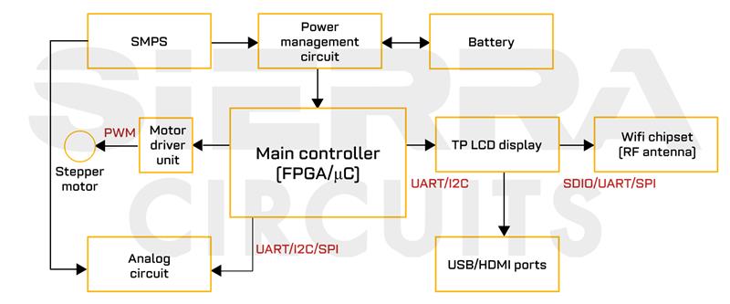
In the above example, we have supplied the microcontroller with a clock signal, and the output is a pulse-width modulated signal. The driver IC then converts the PWM signal into an analog waveform fed to the motors.
UART, I2C, SPI, and SDIO protocols communicate between digital sections, as shown in the above image.
To learn more about interfaces, see a complete guide to PCB interfaces and communication protocols.
Step 3: Enhance ADC functionality
ADC converts analog signals into digital data for processing. Their integration requires careful consideration of factors like resolution, sampling rate, and noise immunity. Proper placement and stable reference clocks are essential to ensure accurate and reliable signal conversion.
3.1 Select the right ADC for your design
When selecting an ADC, consider these 6 parameters:
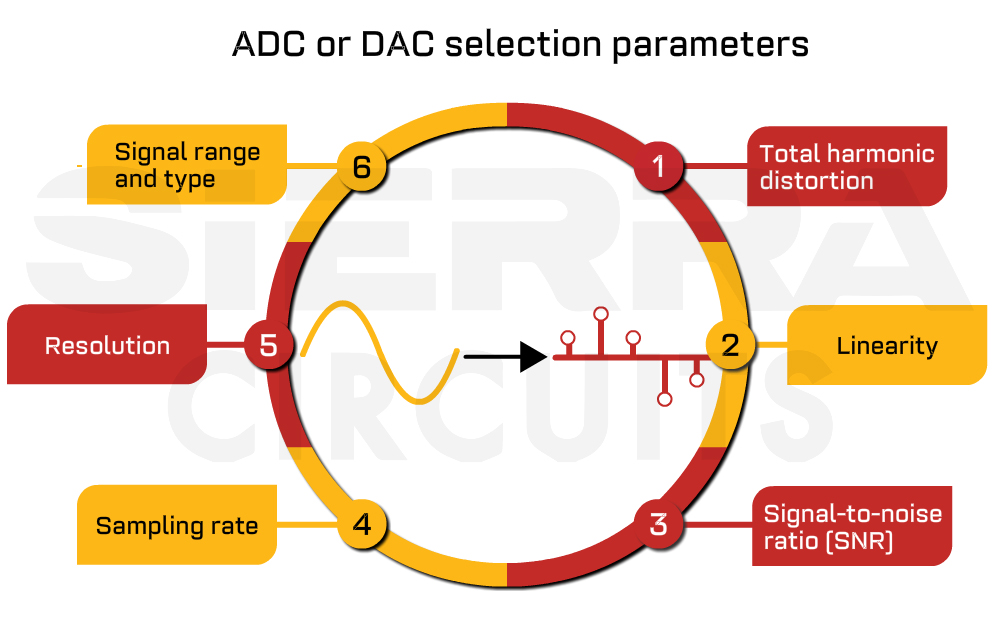
1. Total harmonic distortion (THD): THD measures the distortion introduced by the ADC to the fundamental frequency of the input signal. It is particularly relevant in audio applications, where low distortion is essential for maintaining sound quality.
THD is expressed as a percentage, with lower values indicating better performance. Evaluating the THD specification is essential for applications where fidelity and linearity are crucial, such as audio and video processing.
2. Linearity of ADC: This reflects how accurately the ADC’s actual transfer function aligns with an ideal linear function. It measures how much the ADC’s output values deviate from a straight line, representing the ideal transfer characteristic.
This attribute is particularly important in applications that require precise signal amplitude reproduction, such as audio processing, measurement, and communications.
3. Signal-to-noise ratio (SNR): It measures how much noise affects the signal being processed. It is defined as the ratio of the signal power to the noise power, typically expressed in decibels (dB).
A higher SNR indicates a clearer and more reliable signal representation. In high-precision applications, such as instrumentation and medical diagnostics, a high SNR is critical to ensure that the desired signal can be accurately distinguished from background noise. When selecting an ADC, consider the SNR in your application’s noise environment to ensure effective performance.
4. Sampling rate: It is the frequency at which the ADC samples the analog input, which significantly affects the accuracy of the digitized signal. This parameter is usually expressed in samples per second (SPS).
According to the Nyquist theorem, the sampling rate should be at least twice the highest frequency present in the input signal to avoid distortion.
5. Resolution: It is defined as the number of bits the converter uses to represent the analog input signal. Higher resolution allows for more precise representations of the input signal. This is particularly important in applications requiring detailed signal analysis, such as audio processing or scientific measurements.
For instance, a 12-bit ADC can distinguish 4096 different levels, whereas a 16-bit ADC can differentiate 65,536 levels. The choice of resolution should match the needs of your application. Excessive resolution may lead to increased cost and power consumption without tangible benefits.
6. Signal level and type: The input range defines the minimum and maximum voltage levels the ADC can accurately convert. It can be a positive integer (0 to 2.5) or vary from negative to positive (± 2.5).
If the input signal exceeds the specified range, it can lead to clipping and irreversible signal loss. Consequently, selecting an ADC with a very wide input range may reduce accuracy due to lower sensitivity. Therefore, ensuring that the ADC’s input range matches the expected signal characteristics is vital for maintaining data integrity.
You can also choose the signal type between single-ended and differential signaling. For smooth integration, you must also consider its interface with the main controller (I2C, SPI).
3.2 Provide stable clock signals
The performance of ADCs depends heavily on precise clocking and sampling rates. A stable clock source with minimal jitter is critical, as it can introduce sampling errors, leading to distortion in the converted signal.
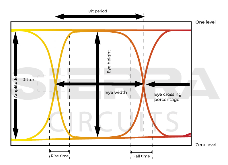
To learn how to minimize jitter in your PCBs, see techniques to measure and avoid jitter in PCBs.
3.3 Isolate noise sources
Since ADCs are sensitive to noise, isolating them from noisy digital components is important. Shielding and careful placement of passive components like capacitors can help reduce noise coupling. Differential signaling may also mitigate common-mode noise and improve signal integrity.
Step 4: Design an efficient stack-up
A reliable PCB stack-up with proper EMI shielding is necessary for mixed-signal designs. An ideal build-up features a ground plane beneath each signal or power layer with short current return paths. If cost constraints prevent this, place signal layers between the ground and power planes to limit inductance.
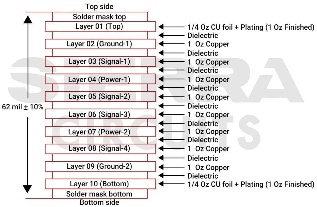
Shorter distances from the signal source to the ground reduce inductance and help contain EMI in your PCB. For instance, stripline signal layers benefit from being sandwiched between ground and power planes creating low equivalent series resistance (ESR) capacitors. This ensures efficient energy storage and delivery, which is essential for maintaining signal integrity and reducing noise.
When routing, ensure signals on adjacent layers are orthogonal to minimize crosstalk and parasitic capacitance.
To learn the steps to build an efficient PCB stack-up, download our eBook.
PCB Stack-Up Design Guide
12 Chapters - 55 Pages - 60 Minute ReadWhat's Inside:
- Design guidelines for HDI, flex, and hybrid stack-ups
- Stack-up representation in fab drawing
- DFM checks for layer stacks
- Characteristics of high-speed materials
- Manufacturing tolerances
- PCB stack-up examples with illustrations
Download Now
Step 5: Implement suitable grounding strategies
Digital circuits tend to introduce noise into the ground plane, negatively impacting the sensitive analog circuitry. This can lead to noise coupling, voltage drops, and signal degradation. When using a single ground plane, it is crucial to ensure that the digital return currents do not interfere with analog ground paths. This approach is simpler to implement but requires careful planning to ensure noise does not propagate across the plane.
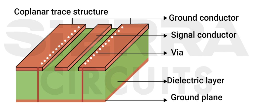
For mixed-signal designs that include RF components, you need to have additional grounding techniques, such as microstrip or coplanar waveguide to ensure proper signal integrity. You can also use shielding and stitching vias to reduce EMI and crosstalk.
Step 6: Optimize power distribution and decoupling
Poor power management can introduce noise and instability. Use separate power planes or rails for analog and digital components. This prevents noise from digital circuits from being introduced into the analog power supply.
6.1 Use dedicated power supplies for digital and analog circuits
The digital supply should exclusively power components placed over the digital ground plane and the analog plane should supply power to the analog and mixed-signal components.
Analog components, especially amplifiers, and ADCs, are sensitive to power supply noise, so you have to use low-noise regulators, filters, and decoupling capacitors to ensure stable power. The digital power supply is less critical regarding noise, but proper decoupling is still necessary to avoid power spikes during high-speed switching.
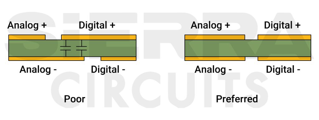
Avoid overlapping digital and analog power planes, which can create unwanted capacitance, leading to RF emissions. Keep the analog supply plane beneath the analog ground plane and the digital supply plane over the digital ground plane to prevent interference.
6.2 Incorporate decoupling capacitors for noise filtering
Decoupling capacitors are essential for filtering out noise from the power supply. Place these capacitors as close as possible to the power pins of each IC to provide immediate filtering and reduce the impact of power supply fluctuations.
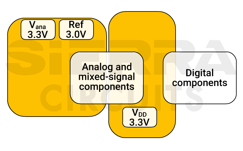
Considering the above example, we have kept the reference voltage for the sensors and ADC as near as possible to the analog section. We have also used Vana of 3.3V to supply voltage to OPAMPS and other components. Select decoupling capacitors to meet the ADC manufacturer’s specifications. Vdd is used for powering the digital circuits.
Step 7: Efficiently route analog and digital traces in mixed signal PCB
When routing both analog and digital signals on the same board, here are the best practices to follow:
- Isolate analog from digital signals. Track and manage all the return paths to ensure there is no interference.
- Use differential pair routing for high-speed signals such as USB, ethernet, or ADC.
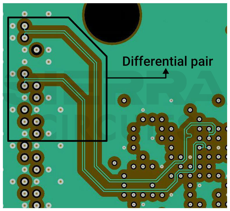
A differential pair routed on a PCB layout. - Ensure the differential pair is length-matched to avoid signal timing mismatch.
- If possible have a solid ground plane adjacent to the high-speed signal to reduce noise.
- Keep sensitive traces from clocks and ADC as short as possible to reduce the risk of signal degradation.
- Avoid routing sensitive traces in the power supply section.
- Do not route over the ground plane split/breaks as it causes a lot of noise.
For more high-speed routing strategies, see 11 best high-speed PCB routing practices.
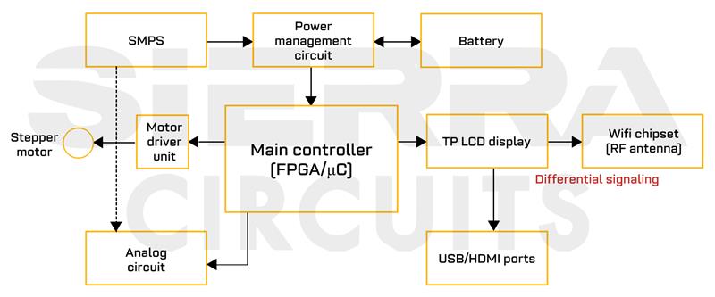
In the above example, the antenna’s RF signals are noise-sensitive. To overcome this challenge, we have implemented differential signaling to route radio traces. You can also route the high-frequency RF signals with controlled impedance and keep them as far as possible from the digital clock and data lines.
Stack-up misalignment can result in incorrect layer thicknesses or dielectric constant mismatches, which can vary the trace impedance. At Sierra Circuits, we use automated scaling software (XACT) that predicts material shrinkage improving the accuracy of the lamination process.
To learn more, visit our RF and microwave PCB manufacturing capabilities.
Step 8: Implement thermal management strategies
Effective PCB thermal management is essential to prevent excessive heat from degrading components and reducing the board’s lifespan. Sensors and ADCs are particularly sensitive to temperature fluctuations. Power consumption is directly correlated with heat generation in both digital and analog sections.
The amount of current consumed by each section can be used to calculate the approximate heat generated. Through your analysis, if the digital section with the microcontroller generates more heat, you can implement forced convection using a fan or provide vents nearby for the airflow.
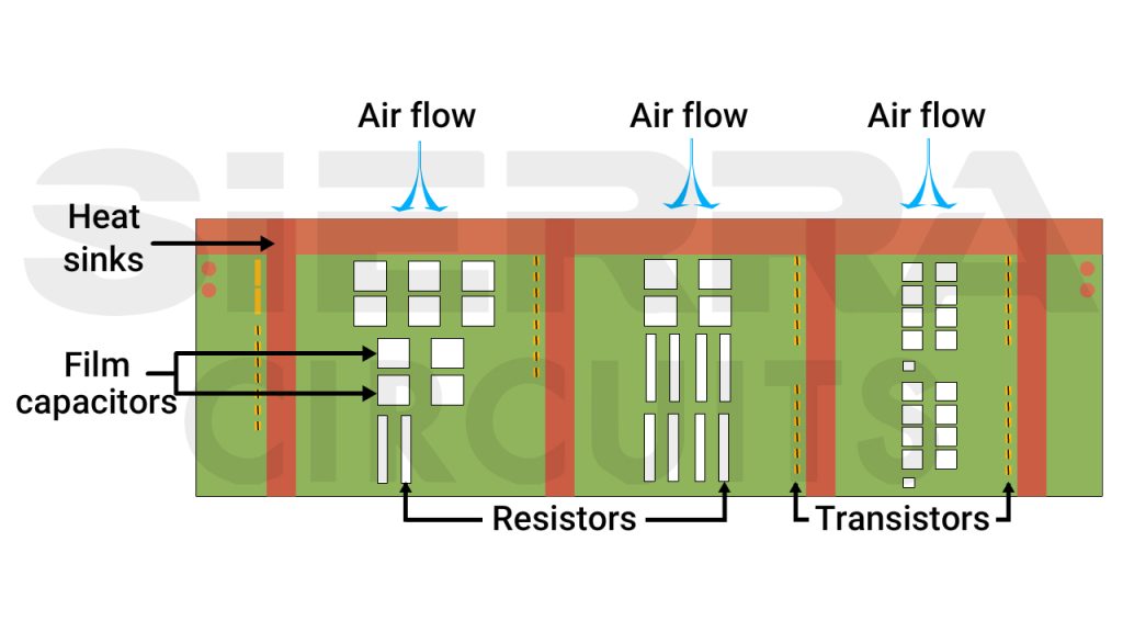
Keep the sensitive analog components away, as excessive heat can cause thermal noise or alter performance. You can also implement heat sinks, thermal vias, and large copper planes to distribute heat evenly across the PCB.
To reduce circuit sensitivity to temperature fluctuations, you can opt for components with more temperature tolerance in other sections. For instance, consider a resistor with R resistance in ambient temperature, and ± Δ will be the variation in its value due to temperature fluctuation.
Implement resistors or capacitors with more tolerance at sensitive components like ADC and sensors to ensure stable performance.
Use thermal simulation tools to predict how heat will be distributed across the PCB. These simulations can help identify potential hotspots and optimize the placement of heat-generating components.
Step 9: Synchronize clock distribution in mixed-signal designs
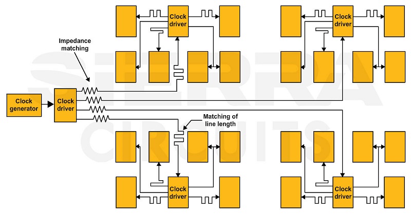
Clock synchronization is critical in mixed-signal designs, particularly when you use multiple clocks.
Consider the sampling clock generation circuitry as an analog section. It requires proper grounding and significant decoupling. You must also isolate it from noisy digital circuits.
Route the clock traces away from noisy components to minimize noise coupling. Use differential clock signals to improve the susceptibility to noise.
If your design utilizes multiple clock domains, synchronize the signals crossing between different clock domains. Techniques like FIFOs (first-in, first-out buffers) or metastability-hardened flip-flops can help manage clock domain crossing.
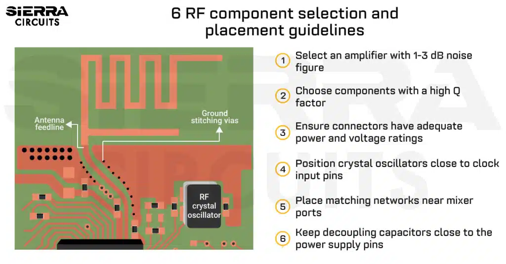
The crystal used for clock generation induces harmonics and EMI. You need to shield these crystals using guard rings. In addition, ground the body of the crystal.
Step 10: Implement shielding for noise management
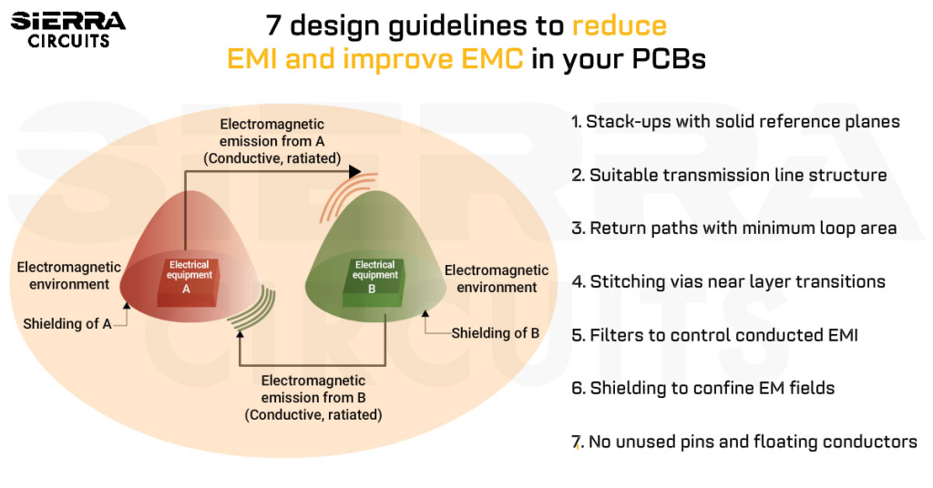
Mixed-signal PCBs often require shielding to protect analog components from digital noise and external electromagnetic interference (EMI).
Signal isolation creates a barrier between different signal paths to prevent unwanted interaction. This is especially critical in systems where noisy digital circuits could corrupt sensitive analog signals.
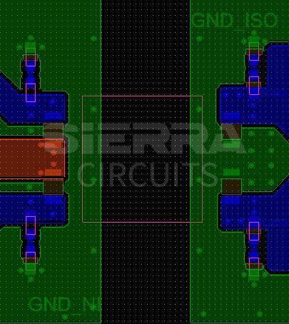
Isolation techniques can include optical isolators, transformers, and capacitive coupling, which effectively separate signal domains while allowing necessary data transfer. By isolating signals, designers can reduce crosstalk and protect sensitive components from voltage spikes or ground loops.

Shielding complements isolation by providing a physical barrier that blocks EMI from external sources. You can achieve this using a Faraday cage, guard rings, or dedicated ground planes.
- Ground planes: A continuous ground plane can shield sensitive analog traces, reducing the influence of nearby digital noise. Additionally, multi-layer boards allow you to place signals on internal layers, which can be sandwiched between ground planes for additional shielding.
- Faraday cages: In some designs, you can enclose sensitive analog circuits in a Faraday cage. It is an electrically conductive enclosure that blocks external electromagnetic fields.
- Guard rings: Guard rings are conductive paths that you can place around sensitive circuit components to minimize interference and enhance noise immunity. They help contain electric fields, reducing the impact of parasitic capacitance and crosstalk.
Step 11: Simulate the mixed-signal PCB design
Once the design is complete, you can ensure the mixed-signal PCB performs as intended through simulations.
- Signal integrity simulation: Tools such as TINA-TI, HyperLynx, or Cadence Sigrity, can analyze the behavior of high-speed digital signals and assess the impact of noise, crosstalk, and signal reflections. These simulations help you identify potential design issues.
- Power integrity simulation: You can use PI simulations to analyze PDN behavior, ensuring that voltage drops, noise, and power supply fluctuations are within acceptable limits. For this, you can use Ansys SIwave or Keysight ADS.
Step 12: Download the production files
When you’re submitting PCB production files to a manufacturer, you ensure proper documentation, accurate data, and clear communication of design intent.
For a mixed PCB design, consider these parameters:
- Board material: Specify the type of circuit board substrate used in the design. Materials with low dielectric loss (such as Rogers) may be necessary for high-frequency mixed-signal designs.
- Copper thickness: Clearly define the copper thickness (e.g., 1 oz/ft², 2 oz/ft²). This affects current handling and thermal properties.
- Impedance control: If your mixed-signal design includes high-speed signals, you may need controlled impedance traces to minimize noise sensitivity. Specify your impedance requirements and tolerances for relevant traces (e.g., 50 Ω for a single-ended trace, 100 Ω for a differential pair).
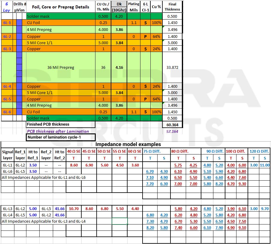
6-layer PCB stack-up with impedance profile. - Shielding and sensitive areas: Indicate areas on the PCB that require extra shielding or have sensitive analog circuitry. If the board includes RF or high-frequency analog circuits, you may need to specify shielded areas or ground fill requirements.
- Via management: Ensure you clearly define the blind, buried, and through-hole vias in the drill files. For mixed-signal designs, controlled via structures (e.g., via stitching for ground planes) might be necessary to manage noise and ensure proper grounding.
Ensure you mark the test points for critical signals in the Gerber files or the assembly drawing. The manufacturer should be able to easily access these test points for functional testing, especially for sensitive analog signals and high-speed digital lines.
Tests conducted for mixed-signal PCBs
Functionality test: It ensures both analog and digital sections operate as intended and interact correctly. The process involves verifying power supply checks such as loading, short circuit, ripple, etc. Checking analog signal paths for noise or distortion.
Testing digital signal circuitry for functionality checks, including a clock, skew, reset, and data lines. Cross-domain interactions, such as noise from digital components affecting analog performance, are closely monitored.
Environmental stress test: It confirms the PCB’s reliability in real-world conditions. The goal is to identify issues before full-scale production or deployment.
EMI test: helps ensure your design meets regulatory standards. These boards are especially susceptible to EMI issues, so shielding and grounding strategies should be validated during this stage.
Mixed-signal PCB design challenges and how to overcome them
4.1 Switching noise causes ground bounce
Switching noise occurs when digital signals transition between states, generating high-frequency noise that can couple into sensitive analog circuits. These transitions trigger a high instantaneous current, leading to ground bounce.
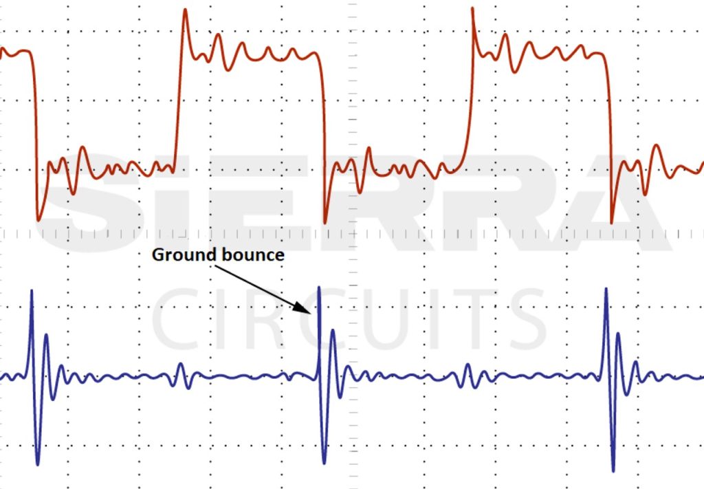
The major sources of switching noise are simultaneous switching I/Os, on-board clocks, and switching regulators. To mitigate this, you must isolate analog and digital traces, implement bypass capacitors, and use effective grounding strategies.
Additionally, filtering methods can help reduce the impact of switching noise on overall circuit performance.
4.2 Ground loops induce noise in the system
When you separate analog and digital grounds, the unintended signal crossover between them will create issues. A ground loop occurs when there are multiple grounding paths, leading to differences in voltage levels that can introduce noise into the system.
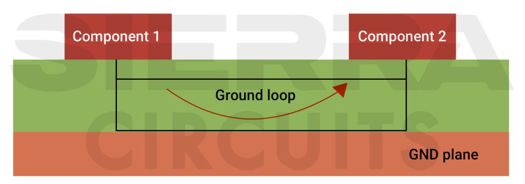
This noise can adversely affect the performance of both analog and digital circuits, resulting in distorted signals. To minimize ground loops, establish a single-point ground reference and isolate analog and digital ground planes.
4.3 Crosstalk results in analog signal errors
Crosstalk arises when unwanted signals are coupled between adjacent traces or components. This interference can degrade signal quality, particularly in sensitive analog circuits. This can create errors in the readings or even performance issues.
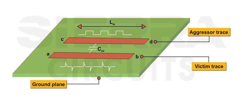
To mitigate crosstalk, PCB designers should maintain adequate spacing between high-speed digital and analog traces, use ground planes for shielding, and implement differential signaling where possible.
Mixed-signal designs may need to meet stricter regulatory standards for emissions and interference, adding another layer of complexity to the design process.
Key takeaways
- Segregate analog and digital sections.
- Understand the different communication protocol requirements.
- Choose ADCs with appropriate resolution, input range, and sampling rate for your application.
- Use a ground plane beneath signal and power layers for effective EMI shielding.
- Plan return paths carefully to reduce noise propagation.
- Use separate power planes or rails for analog and digital sections.
- Avoid routing traces over split ground planes and through power supply areas.
- Keep sensitive analog components away from heat sources.
- Synchronize multiple clock domains with techniques like FIFOs or metastability-hardened flip-flops.
- Shield sensitive components with Faraday cages, ground planes, and guard rings.
- Perform signal integrity (SI) simulations to address noise, crosstalk, and reflections.
- Specify board materials, copper thickness, impedance control, and shielding requirements in the production files.
Mixed-signal PCB design requires careful attention to circuit isolation, grounding, routing, and power supply management. By following the best practices discussed in this article, you can ensure you can avoid noise and interference in your mixed-signal layouts.
Whether designing a simple sensor system or a complex data acquisition board, these principles will help you navigate mixed-signal design challenges and create robust, high-performance PCBs.
About Sushmitha V : Sushmitha V has a master's degree in power electronics and has over four years of experience in the PCB industry. Her areas of interest include circuit board manufacturing, assembly, IPC standards, and DFM/DFA practices.







How do I determine the best way to partition analog and digital sections?
What considerations are crucial for clock placement?
To partition analog and digital sections effectively, physically separate them on the PCB. Assign dedicated areas for each, minimizing overlap. For multilayer designs, allocate separate layers for analog and digital sections.
Keep high-frequency digital signals, such as clocks, away from sensitive analog circuits. Route analog signals with minimal trace length and avoid crossing noisy digital paths. Consider using shielding, filtering, and proper decoupling to prevent interference. This strategy ensures signal integrity and reduces noise.
When placing clocks in a mixed-signal PCB design, position them as far as possible from analog circuits to minimize noise interference. Use short, direct signal paths for clock traces to reduce signal degradation and minimize the impact of parasitic inductance. Consider the use of shielded traces or ground pours around the clock trace to isolate it further.
Ensure proper termination and impedance matching to avoid reflections and maintain signal integrity. Finally, ensure that any clock-related components like buffers or drivers are placed close to the clock source to maintain timing accuracy.