


Contents

On-demand webinar
How Good is My Shield? An Introduction to Transfer Impedance and Shielding Effectiveness
by Karen Burnham
In a modular PCB design method, a complex circuit board is divided into smaller modules. Each performs a specific function and can be tested independently. This optimizes the layout creation process, cuts down the design turnaround time, and helps manage complexities.
By breaking down a board layout into smaller and functional units, engineers can streamline the design process, enhance scalability, and improve collaboration.
Highlights:
Steps to modularize a PCB design:
- Identify and group functional units based on signal flow, power distribution, physical constraints, and complexity balance.
- Create schematics, choose components, and interconnect each module separately to simplify routing and minimize interference.
- Collaborate with version control systems, conduct regular reviews, and utilize real-time co-editing tools.
- Define the individual or team’s role at different stages of the design process.
In this article, you will learn the steps involved in a modular PCB design.
What is a modular PCB design?
Transforming a complex design concept into an actual layout involves multiple intricate steps. Without a well-planned approach, even a minor issue can lead to design rework, wasting valuable time and effort.
This is where the PCB modularization technique comes in. It breaks down complicated networks into small functional blocks, allowing you to keep track of your design and minimize errors.
Each block represents a subsystem of the circuit board. These modules can be developed, tested, and optimized independently before being integrated into your PCB layout.

When should you implement a modular PCB method?
Opt for a modular PCB design when you’re working on:
- Embedded systems: They often integrate multiple functionalities, such as sensors, actuators, communication units, and user interfaces. A modular PCB design allows each function to be developed and tested as a separate module, simplifying the overall design process and ensuring better reliability.
- Multi-board systems: These include several interconnected PCBs, each handling specific functions like power management, data processing, and communication. The modular design helps manage these interconnections efficiently, ensuring that each board functions correctly both independently and as part of the overall system.

- Mixed-signal circuits: They require careful analog and digital signal management to prevent noise and interference. Breaking the board into sections allows for physical and electrical isolation of these circuits, enhancing signal integrity and system performance.
For tips on reducing EMI in your layout, see 7 tips and PCB guidelines for EMI and EMC.
How different teams collaborate to complete a PCB design project

Understanding modularization as a cross-functional effort is essential. All the involved stakeholders must collaborate seamlessly to achieve high-quality outcomes in each stage of the design process. Here’s how different teams collaborate at each phase:
| Design stage | Stakeholders | Process |
|---|---|---|
| Initial consultation and information gathering | Design lead, project manager, and client | The design lead and project manager discuss layout requirements with the client to understand the scope, goals, and specifications. This helps develop a clear plan and timeline for the project. At this stage, they will decide what modules to create and define every team members' responsibilities. The design lead will be the single point of contact for the client. |
| Schematic design | Layout engineers/ design engineers | Engineers collaborate to create a schematic that meets the project requirements. They discuss design choices, component selection, and circuit layout to ensure an optimal and error-free design. |
| Footprint and library creation | Footprint designers and layout engineers | Footprint designers create component footprints based on the schematic provided by the layout engineers. They collaborate to ensure components are standardized and adhere to the industry guidelines. |
| Stack-up design | Layout engineers and manufacturing experts | Layout engineers are primarily responsible for determining the signal integrity requirements of the PCB, including impedance control, signal routing, and power distribution. They define the layer stack-up configuration that best meets the electrical performance criteria of the design. Manufacturing experts play a crucial role in selecting the appropriate materials and manufacturing processes for the stack-up. They make sure the stack-up can be manufactured within the specified time and cost. |
| Component and material sourcing | Procurement specialists/inventory managers and layout engineers | Procurement specialists are responsible for sourcing components, materials, and services needed for fabrication and assembly. They identify suppliers, negotiate contracts, and ensure that components meet quality and reliability standards. They are also responsible for managing stock levels and inventory turnover. Layout engineers specify the components and materials required for the circuit design. They collaborate with procurement specialists to identify suitable components, ensure availability, and address technical or compatibility issues, if any. |
| Layout design | Design lead and layout engineers | Layout engineers design the assigned sections according to the design requirements, focusing on signal integrity, thermal management, and manufacturability. They use placement and routing strategies to minimize errors and maximize performance. They integrate the designed sections and use simulation tools to detect potential issues. |
| DFM and DRC checks | Layout engineers, DFM specialists, and manufacturing experts | Layout engineers work with DFM specialists to ensure the design meets manufacturability standards and avoids common pitfalls. They also perform design rule checks to identify and rectify potential issues. Later, designers generate production files and work with manufacturing experts to ensure files meet production standards. This includes reviewing Gerber files, drill files, and assembly drawings. |
| Client review and feedback | Project manager, design lead, and client | The design team presents the completed design to the client for review and feedback. The project manager facilitates communication between the team and the client to address any changes or concerns. Based on the client feedback, designers make any necessary revisions. Once the design is finalized, it is sent for production. |
To learn how to build a perfect PCB stack-up. Download our design guide.
PCB Stack-Up Design Guide
12 Chapters - 55 Pages - 60 Minute ReadWhat's Inside:
- Design guidelines for HDI, flex, and hybrid stack-ups
- Stack-up representation in fab drawing
- DFM checks for layer stacks
- Characteristics of high-speed materials
- Manufacturing tolerances
- PCB stack-up examples with illustrations
Download Now
Step-by-step process of creating a modular board design
In this technique, you need to start by grouping sections and defining interfaces. Next, create the design modules and test them individually before integrating them. Finally, test the entire board to ensure all the modules are accurately connected. Here’s how the modular PCB design process works:
Step 1: Break down the design into functional units

Group the design modules based on their functionalities, such as power supply, communication interfaces, and analog and digital logic circuits.
On the other hand, factors like heat dissipation, physical constraint, and signal speed can also be used to segregate the sections. The factors to consider during modularization include:
- Functional units: Determine the device’s main functions and subsystems. For example, a digital camera might have modules for image sensor, image processing, power management, user interface, etc. The main unit is the image processing system, which performs color correction and noise reduction. Power management circuits, image sensors, and user interfaces are subsystems.
- Signal flow: Consider how signals flow through different modules. Place the units that share common signals close to each other.
- Power distribution: Check each module’s power requirements. Group sections that share the same power supply.
- Physical constraints: Consider the PCB’s physical layout, including size constraints and mounting locations. You can organize modules based on spatial proximity or physical connectivity.
- Design complexity: Aim for a balance between module complexity and simplicity. Avoid creating too large or too small modules, as this can make the design overly complex or fragmented.
In unique instances, modules can be arranged on different boards. Having separate boards can increase the number of components and project costs. However, when there is a space constraint or the design demands physical signal isolation, this can become an elegant solution.
The divided boards can be stacked like a multi-board system or even mounted at separate locations and connected through cables.

For example, Sierra Circuits’ PCB design team engineered a circular board for one of our clients. The client didn’t initially consider the space constraint in the application and wasn’t able to mount the board as per the product design. We suggested splitting the board into two semicircles and connecting them through cables. This idea was successful, and the board was installed without a hitch.
If you would like us to design PCB layouts for you, talk to our PCB design experts for a tailored solution.

Step 2: Create schematics for each functional unit

After identifying each functional unit and defining its requirements, you can create the schematic. Keep these 10 things in mind when creating a schematic:
- Choose appropriate components for each functional unit. Ensure components are compatible with the overall system requirements and available in the market.
- Ensure pin configurations and connector types are standardized across modules.
- Create separate schematic sheets for each functional unit. Link these sheets hierarchically to represent the board’s modular structure. Most EDA tools like Altium Designer, Zuken, Cadence Allegro, and KiCad have this feature.
- Clearly define the interfaces between sections, including signal connections, power distribution, and communication protocols. This ensures proper integration and communication between modules.
- Specify the breakdown of modules in the PCB design documentation. This helps maintain consistency throughout the design process and facilitates collaboration among team members.
- Import the verified schematics into the EDA tool for layout creation. Using the co-editing option, multiple team members can collaborate on the project simultaneously.
- Ensure that power and ground planes are accurately designed to minimize noise and provide stable power distribution.
- Place the components of each functional unit in their designated areas.
- Route the signals within each functional unit. Pay special attention to high-speed signals, differential pairs, and impedance-controlled traces. Learn about common PCB design challenges and practical solutions in our blog, 5 typical PCB design challenges with solutions for engineers.
- Ensure the traces are as short as possible to minimize signal delay and potential interference.
For schematic design guidelines, see how to draw and design a schematic.
For step-by-step guidelines on designing a high-speed PCB, download our eBook.

High-Speed PCB Design Guide
8 Chapters - 115 Pages - 150 Minute ReadWhat's Inside:
- Explanations of signal integrity issues
- Understanding transmission lines and controlled impedance
- Selection process of high-speed PCB materials
- High-speed layout guidelines
Download Now
Step 3: Collaborate through tracking versions and design reviews
A successful collaboration is only possible by sharing precise information between teams. Here are the things a PCB design team should ensure to collaborate seamlessly:
Version control system: Tracking design changes becomes crucial when multiple people collaborate on the same project. Without a clear version control system in place, there’s a risk of using outdated module versions. To avoid this, maintaining a history of changes is critical for identifying and resolving issues efficiently.
Regular design reviews: With regular review meetings, all team members will receive a status update and promote knowledge sharing. This will help identify problems in the early stages and improve design integrity.
Collaboration tools and software: With the current technological upgrades, many EDA tools like Altium Designer, Zuken, Cadence Allegro, and KiCad provide real-time co-editing options where multiple members can work on the project simultaneously. You can have shared libraries of components, symbols, and footprints for consistency across the design.
Cloud platforms allow users to access files from anywhere and through any device, facilitating global collaboration. Many teamwork management tools, such as Trello, Asana, and Atlassian, help you to improve communication and documentation.
Use the Better DFM tool to identify potential manufacturing issues in your design.
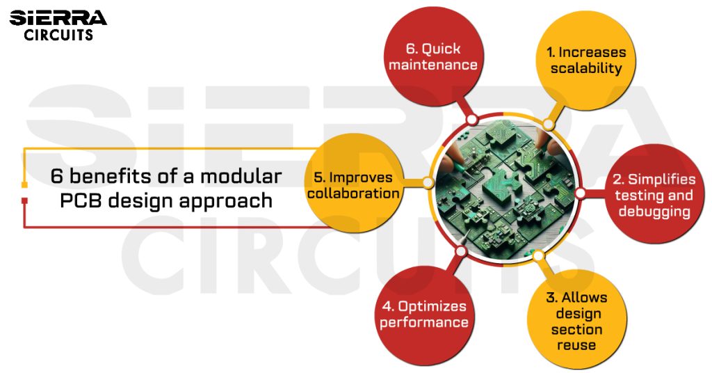
6 benefits of a PCB design modularization
1. Improves scalability
This method allows for easy scalability, as individual sections can be added, removed, or modified without affecting the entire layout. It facilitates design adaptation to the changing requirements or specifications.
2. Simplifies testing and debugging
Smaller modules make testing and debugging hassle-free. PCB engineers can isolate and troubleshoot issues in a section without affecting the entire system’s functionality.
3. Allows module reuse
The modular design promotes block reuse. You can create layout sections to be independent and interchangeable. Leveraging previously validated modules across different projects or iterations reduces design time, effort, and the risk of errors.
For more, see autogrouping for repetitive design blocks.
4. Facilitates quick maintenance
Any failed or outdated modules can be quickly replaced or upgraded without any extensive rework, minimizing downtime and reducing costs.
5. Improves collaboration
Modular PCB design encourages effective collaboration among team members. Here, different engineers can work on individual modules concurrently. This accelerates the design process and allows specialization in specific areas of expertise.
6. Optimizes performance
This approach enables designers to focus on maximizing the performance of individual modules, leading to improved overall system performance. By optimizing each module independently, designers can achieve better efficiency, reliability, and signal integrity.
From design concept to prototype, Sierra Circuits can assist you in every step. Visit our PCB design services to learn more.
Key takeaways:
- The modular design minimizes the risk of errors and costly redesigns by breaking down complex networks into smaller blocks.
- This method facilitates quick replacement or upgrading of modules and reduces downtime and maintenance costs.
- It promotes the reuse of previously validated modules, saving design time and reducing the risk of errors.
- Effective isolation and management of power circuits and signals for improved performance.
- Supports quicker iterations and revisions during the prototyping stage, speeding up time-to-market.
- Encourages team collaboration with different engineers specializing in specific areas, improving design quality and efficiency.
Creating functional units in modular PCB design involves meticulous planning and execution during both the schematic and layout design stages. By breaking the design into manageable blocks, engineers can streamline the design process, ensure higher reliability, and facilitate easier upgrades and maintenance. This modular approach is especially beneficial in complex projects, significantly enhancing efficiency and productivity.

About Sushmitha V : Sushmitha V has a master's degree in power electronics and has over four years of experience in the PCB industry. Her areas of interest include circuit board manufacturing, assembly, IPC standards, and DFM/DFA practices.


Start the discussion at sierraconnect.protoexpress.com