Contents

On-demand webinar
How Good is My Shield? An Introduction to Transfer Impedance and Shielding Effectiveness
by Karen Burnham
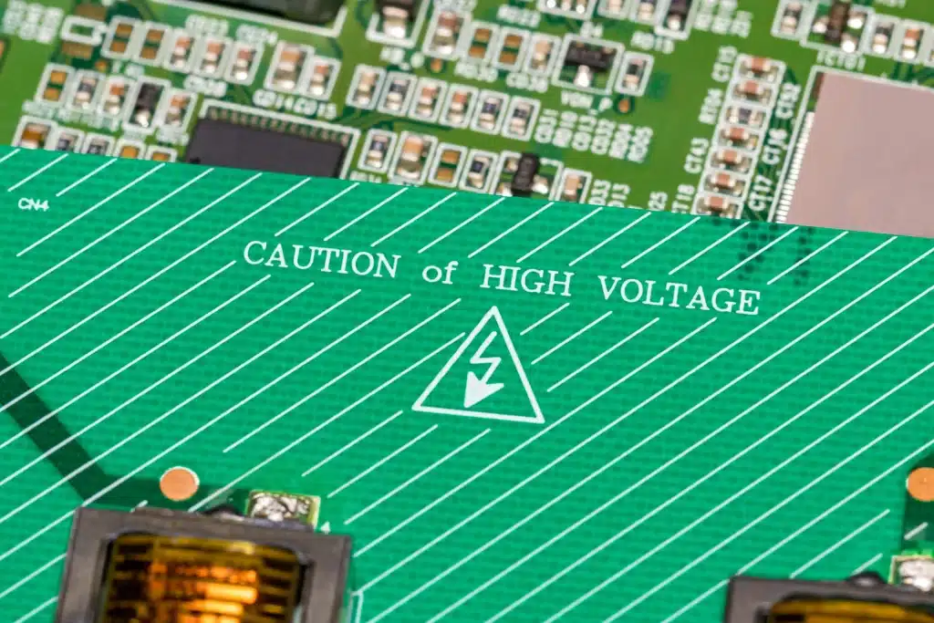
While dealing with high voltage circuit boards, remember the basic rules for laying out the boards is that they will carry hazardous voltages.
High voltage board designing requires an understanding of international safety standards such as IPC 2221A and UL 60950-1. In this article, you will be learning some critical considerations important from a high voltage PCB design angle.
Creepage and clearance considerations in high voltage circuit boards
The system or product for which your board is destined must meet IEC or UL standards. The minimum distance permitted between conductors that are subject to hazardous voltage will include a wide margin for safety, which depends on:
- The peak working voltage and the laminate material. Read our article on how to choose PCB materials and laminates for fabrication.
- The operating environment (moisture, particulates, and altitude).
- The circuit location relative to human access or proximity, and whether the traces involved are on an internal or outer layer?
- The spacing required on outer layers also depends on whether traces are coated or bare. Read our case study on designing a high-current PCB with voltage doublers, where we calculate conductor spacing for the internal and external layers with conformal coating for different voltage pulses.
If the clearance is too small, a transient over-voltage event can result in arcing between the conductors. This is a virtually instantaneous fault that does not recur until another such over-voltage event. Faults resulting from insufficient spacing for creepage can take much longer to occur.
Determining what spacing to use is simple if your system or product requires compliance with international safety standards. Find the standard relevant to the product category and adhere to the tabulated values concerning your application’s details. For example, IEC-60950-1 (second edition) is the document to consult for most IT products to be sold internationally that are powered from AC mains or batteries and applies both to the primary side and the DC secondary circuits within those products. Section 2.10.3 of the standard defines what clearances are required. So, that over-voltages, including transients and peak voltages generated within the equipment, cannot cause faults. A series of tables, 2J through 2M, explains how to calculate clearances with respect to the details of your application. Next, section 2.10.4 explains how to determine the spacing required for creepage. Check our post on the importance of PCB line spacing for creepage and clearance for more insight.
PCB Material Design Guide
9 Chapters - 30 Pages - 40 Minute ReadWhat's Inside:
- Basic properties of the dielectric material to be considered
- Signal loss in PCB substrates
- Copper foil selection
- Key considerations for choosing PCB materials
Download Now
Clearance vs. creepage in high voltage circuits
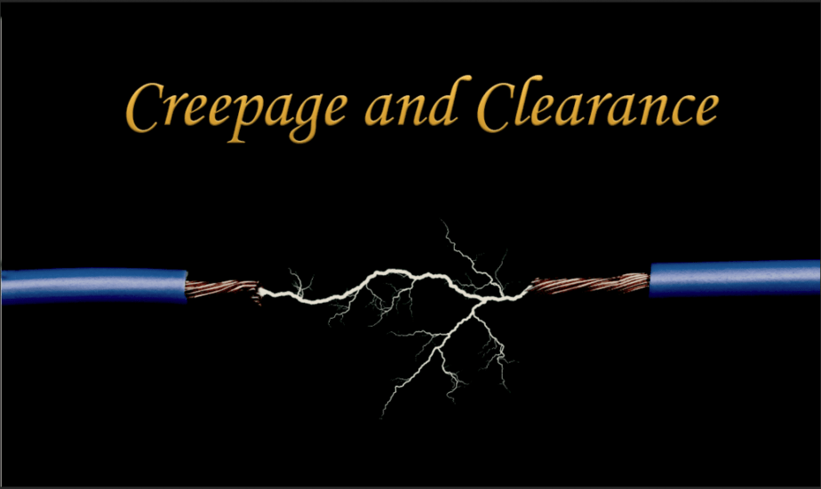
What is the difference between clearance and creepage? Clearance is the shortest distance between two conductors measured through air. Creepage is the shortest distance between two conductors, measured along the surface of the insulation separating them. An electrical fault between conductors can occur if the clearance or the creepage spacing is too small. If the clearance is too small, a transient over-voltage event can result in arcing between the conductors, especially if there is dust in the air or humidity. This is a virtually instantaneous fault that does not recur until another such over-voltage event. Faults resulting from insufficient spacing for creepage can take much longer to occur.
Over time, usually stemming from dust buildup and moisture, a path (in other words, a track) for current to leak from one conductor to another, can develop and cause a gradual breakdown of the surface of the insulating material between them. The mechanism for this is not a voltage spike—though that could contribute—but the continual presence of high voltage combined with an insulating material whose Comparative Tracking Index (CTI) is too low.
CTI is a measure of a material as an electrical insulator and is expressed as the voltage at which the surface of material breaks down under a standardized test. The manufacturers of PCB laminates publish CTI figures for their products. For convenience, the breakdown voltages are divided into six categories: The highest rating is 0 for withstanding values of 600V and greater, and the lowest is 5 for less than 100V. For example, conventional FR4 has a comparative tracking index of 175 to 249V, which places it in category 3.
Read 4 common PDN design challenges and how to resolve them to learn how to improve the efficiency of power distribution in high-voltage circuit boards.
Safety standards for high voltage circuits
The paramount objective of all electrical safety standards is to prevent any danger of shock. Suppose no one will ever be near a circuit while it is powered. In that case, the clearance and creepage allowances among its conductors that are subject to hazardous voltage can be the minimum that ensures the circuit will function and not deteriorate. IEC-60950-1 specifies five increasing levels of mandatory insulation related to the physical location of a circuit relative to human contact, the voltage, and the operating environment. Naturally, the best tactic to avoid the danger of shock or circuit degradation is to space traces as far apart as possible, but very often, that distance will not meet creepage requirements. What can be done in those cases?
If turning to a material with a better CTI is not feasible, routing a slot in the space between two traces can increase the creepage distance. Leakage from one trace to the other along the laminate surface would have to travel around the air gap. Alternatively, a vertical barrier of insulating material could be placed in the space, which would increase both the creepage and clearance distances.
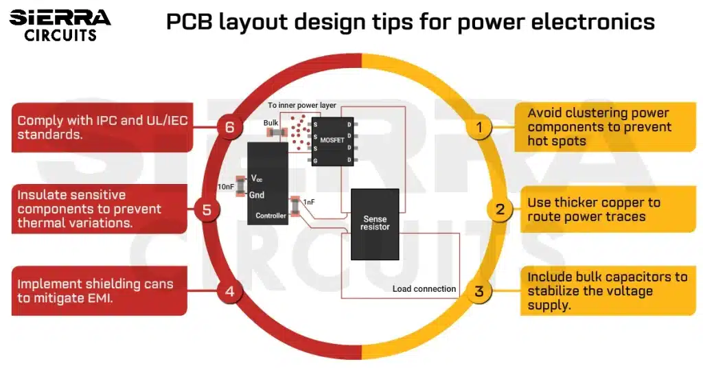
For more power electronics safety considerations, see 7 PCB layout design tips for power electronics.
Keep in mind the spacing on assembled high voltage circuit boards when you consider creepage and clearance requirements for layout. The distance between an uninsulated edge of a charged component and the edge of an adjacent component could be too small to meet a clearance requirement, even though the creepage distance between their traces is sufficient. Moreover, there may be some operations needed during assembly to meet clearance requirements. For example, applying the potting compound to isolate the leads on the package of a power semiconductor from some nearby component.
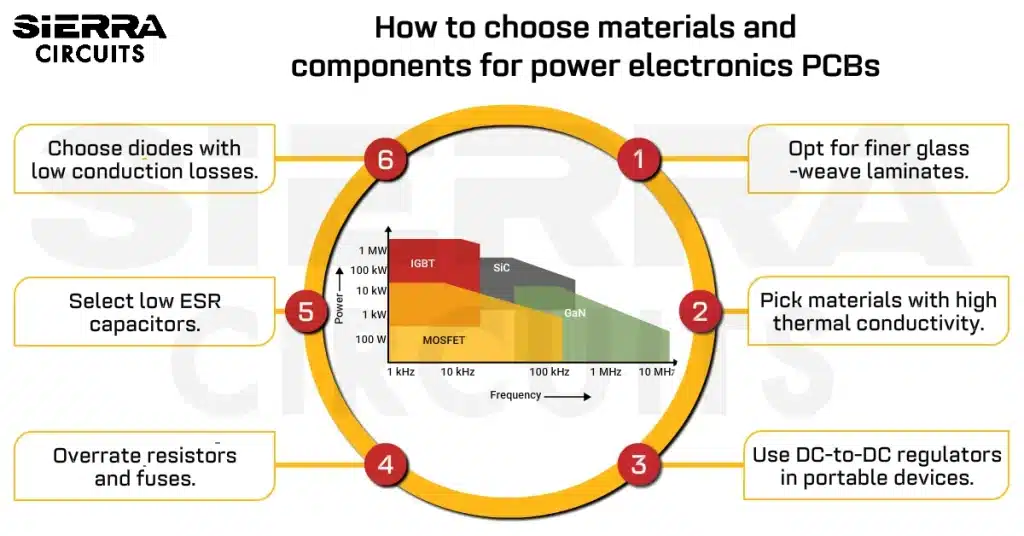
To learn how to pick the right parts for your high voltage board, see how to select components and materials for power electronics PCBs.
If your project does not require compliance with a particular safety standard, you can rely on the latest version of IPC-2221, the generic standard for PCB design, for clearance and creepage guidance. In any case, consultation with your PCB fabricator and assembler regarding suitable materials (you can read our article on how to choose HDI PCB materials) and design alternatives will help you achieve a safe product that meets your performance objectives at the lowest possible cost.
Our quick trip through the basics of laying out the high voltage circuit boards that involve hazardous voltage amounts is simply an opportunity to point out some helpful and hopefully familiar guideposts as you start your journey.

Design for Manufacturing Handbook
10 Chapters - 40 Pages - 45 Minute ReadWhat's Inside:
- Annular rings: avoid drill breakouts
- Vias: optimize your design
- Trace width and space: follow the best practices
- Solder mask and silkscreen: get the must-knows
Download Now
Creepage and clearance in high voltage circuit boards are the essential parts of all safety measures. That is why it is mandatory for the design engineers to meet the product safety standards throughout the entire design stage to avoid any chances of failure. The concept of creepage and clearance not only applies to the PCB but also to the components placed on it.


