Contents

On-demand webinar
How Good is My Shield? An Introduction to Transfer Impedance and Shielding Effectiveness
by Karen Burnham
Syed Ubaid Ali Warsi, the owner of Wavetroniks, provided his insights into high-speed and HDI PCB design strategies at PCB West 2023. Syed is an expert in high-speed designs and an EMC consultant.
Highlights:
- Choose Megtron 6 for high-speed applications such as NRZ and PAM4 to lower the signal losses.
- Utilize the design reuse function in your designs to save time.
Watch the full video to learn more.
What is the one rule a designer should follow to maintain signal integrity in high-speed designs?
Syed Ubaid Ali Warsi: Signal integrity becomes a crucial factor when dealing with high-speed designs. The fundamental goal is to ensure that your signal traces don’t encounter any unwanted reflections. This can be achieved by consistently maintaining the impedance across your traces.
It applies from the source to the load through the transmission line. When impedance mismatches occur, it can lead to EMI issues and data errors at the load end. To ensure a smooth operation, check the material/component data sheets to determine the specified impedance values and how to properly control them.
High-Speed PCB Design Guide
8 Chapters - 115 Pages - 150 Minute ReadWhat's Inside:
- Explanations of signal integrity issues
- Understanding transmission lines and controlled impedance
- Selection process of high-speed PCB materials
- High-speed layout guidelines
Download Now
Does tight coupling of differential traces help prevent EMI and crosstalk?
Syed Ubaid Ali Warsi: Indeed, when we talk about tight coupling, the question arises: why use differential pairs? The answer is that in differential pairs, the signals traverse with two polarities, positive and negative. When we run these signals side by side with tight coupling, it effectively cancels out common mode noise, which is a primary source of EMI. This is why we opt for tight coupling in running differential pairs.
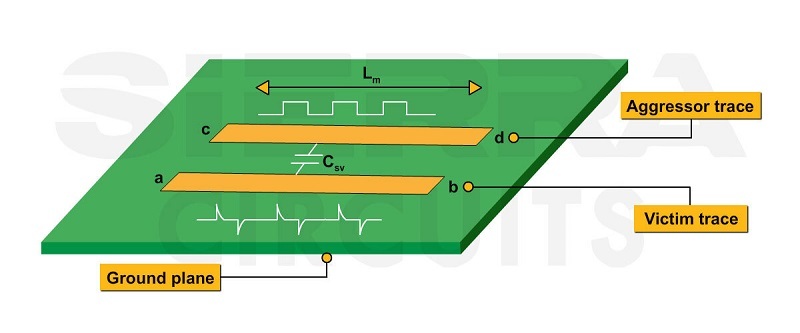
To learn more crosstalk prevention techniques, see handle crosstalk in high-speed PCB designs.
What are the HDI PCB design considerations for fine-pitch components and microvias?
Syed Ubaid Ali Warsi: HDI is a whole different world. In recent times, we’ve witnessed packages shrinking from 1 mm pitch to 0.8 mm, and now we’re even down to 0.3 mm and 0.2 mm.
When working on high-speed and HDI PCB designs, the initial strategy is to check whether your envisioned design is feasible for fabrication. To facilitate this, engage with your PCB fab house in the design stage. Consulting them provides invaluable insights into constraints you should be looking at. Further, you can learn how to break out your system effectively.
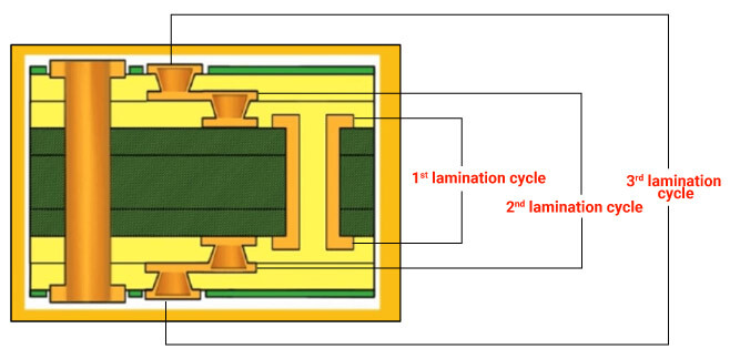
You should also consider factors like microvias and laser vias. Determine the number of sequential lamination cycles you’ll need. You may require a simple HDI PCB with microvias on the outer layers and a central buildup layer. You can also opt for a complex interconnect design structure. These considerations are vital when dealing with high-density PCB designs.
What are some common EMC-related issues you’ve encountered in your career, and how did you resolve them?
Syed Ubaid Ali Warsi: When we talk about EMC, we are referring to the entire system, which may include multiple PCBs within it. These boards are integrated into a modular system, culminating in a complete system that undergoes EMC testing.
The right stack-up can often resolve these issues effectively. A wider stack-up (layer stack with a higher number of layers or greater thickness) can help mitigate most EMC problems.
You need to ensure minimal spacing between your power and ground planes. Sometimes, you unintentionally create a significant gap between the power and ground planes. As a result, this large spacing results in poor decoupling and affects the performance of your PDN.
To maintain a low PDN impedance, tightly couple your power and ground planes in the build-up. It can effectively address many EMC issues, making it a crucial consideration.
Can you discuss the challenges and strategies involved in designing boards with 0.2 mm CSP (chip-scale package) multi-lamination break-outs?
Syed Ubaid Ali Warsi: When working on 0.2 mm CSP packages, we use a break-out package. This package transforms the 0.2 mm CSP into a more manageable 0.8 mm interposer. This way, you don’t have to handle the 0.2 mm devices directly, making the process much simpler.
The challenge here is to identify a suitable vendor or fab house to manufacture your products. This is because we’re dealing with 3- 4 lamination cycles with stacked and staggered vias. This can pose manufacturing yield issues.
Unfortunately, when working with HDI PCBs, achieving a high yield is not easy. This is the reason they tend to be expensive; you’re essentially paying more due to the lower yield in the manufacturing process.
Additionally, there’s the complexity of dealing with fine features, such as a 3-mil trace spacing. The size of the vias used for the laser drill is also around 3 mil, which presents a significant challenge.
HDI PCB Design Guide
5 Chapters - 52 Pages - 60 Minute ReadWhat's Inside:
- Planning your stack-up and microvia structure
- Choosing the right materials
- Signal integrity and controlled impedance in HDI
- Manufacturing considerations for higher yields
Download Now
Can you give us a few pointers on PCB stack-up design for high-speed applications?
Syed Ubaid Ali Warsi: When you are designing a high-speed PCB design, you need to understand your impedance requirements.
There are three key factors to keep in mind: distance between two layers, trace spacing, and trace width.
When it comes to material selection, you need to choose a material with low Dk. For applications like NRZ and PAM4, prefer Megtron 6 material. It offers a low signal loss.
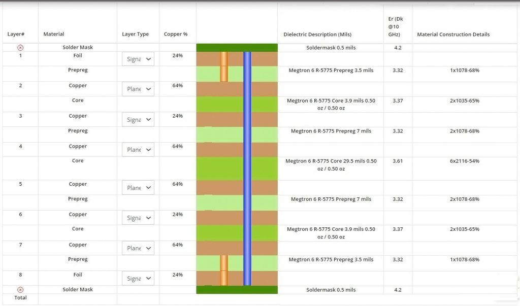
Furthermore, it’s essential to pay attention to the weave pattern of the dielectric material. Determine which pattern suits your design best (glass weave or fiber weave).
Could you provide examples of innovative solutions or design techniques you’ve employed in your career?
Syed Ubaid Ali Warsi: When designing a PCB layout, it’s essential to involve a variety of individuals such as hardware designers, PCB layout specialists, mechanical designers, vendors, and the fab assembly house. Bringing them into the process and getting them involved from the outset is crucial for design success. This helps you to deliver the product on time.
One innovative approach that could be extremely valuable is the consistent usage of the design reuse function. This practice should be a staple in our work because, in reality, we frequently use the same circuits. There’s no need to start from scratch when you’ve already designed something before. The key is to identify where you’ve employed a particular design, extract it from there, and reuse it, saving you valuable time.
For example, even in cases like switch mode power supply design, some designers insist on starting from square one. They essentially reinvent the wheel and open the door to potential inconsistencies and problems. It makes more sense to leverage the design that’s been created and tested before. So, the key takeaway here is to make use of the design reuse function and work smarter, not harder.
Another valuable practice for innovative designers is to implement a checklist system. When you initiate a design, create a checklist that outlines the essential parameters to consider.
As you approach the design release stage, make sure that all the boxes in your checklist are ticked. This includes design rule checks (DRC), drill tables, and fabrication notes. In addition, your stack-up should align with what you’ve defined in your CAD tool and fabrication drawings. These are critical elements to incorporate into your design process to ensure a smoother and more reliable outcome.
Key takeaways:
- Engage with your fab house in the initial stage of the design phase to reduce the product development time.
- Maintain minimal spacing between power and ground planes to mitigate EMC issues and maintain a low PDN impedance.
- Implement a thorough checklist system throughout the design process for a reliable PCB.
Implement these techniques suggested by Syed Ubaild Ali Warsi in your next high-speed and HDI projects. It will help you achieve exceptional signal integrity in your PCB designs.




Start the discussion at sierraconnect.protoexpress.com