Contents

On-demand webinar
How Good is My Shield? An Introduction to Transfer Impedance and Shielding Effectiveness
by Karen Burnham
Testing and examining a PCB after manufacturing is a pivotal factor in procuring a flawless design. Design for testing (DFT) evaluates the board’s accuracy based on functionality and manufacturability.
DFT is similar to reviewing your answer copy in an examination just before the final submission. It does require some extra effort and time but eventually, DFT helps in creating an error-free board.
What is design for testing?
DFT is a method of operational and functional testing of a board and layout optimization.
This methodology identifies any short, open circuit, wrong placement of the components, or faulty components. This testing method is performed to validate three major questions:
- Is the board designed precisely?
- Is the board fabricated flawlessly?
- Do all the components, ICs, and connections operate perfectly?
The other major issues considered are:
- Components should be spaced properly to mitigate the risk of defective testing.
- If the solder masks between pads are not provided correctly, the electrical connections can degrade.
- Optimization of drill bit size.
- Improper surface-mount pad size.
Why DFT is required?
In the earlier days, the number of components was hardly around 100 to 200. Hence, the board had enough room to place test points. Now, the entire fabrication technology has gone through a revolutionary change. Some PCB designs include thousands of components and solder connections, especially in HDI boards. The space constraint becomes a concerning issue in deciding proper test positions on a dense board. If any component or connector hampers the design, it would be a nightmare for fabricators and designers.
DFT engineers and product developers establish a set of testing methods to find out any inaccuracies and produce a high-quality, operational circuit board.
Parameters to include in DFT
Here are some of the parameters that you can include in testing to ensure efficiency and precision.
- Test points: Test point insertion is a requisite technique in DFT to increase test efficiency. The position of a test point is decided based on how many components it can cover. The signal integrity issue can be mitigated by arranging accurate power and ground test points.
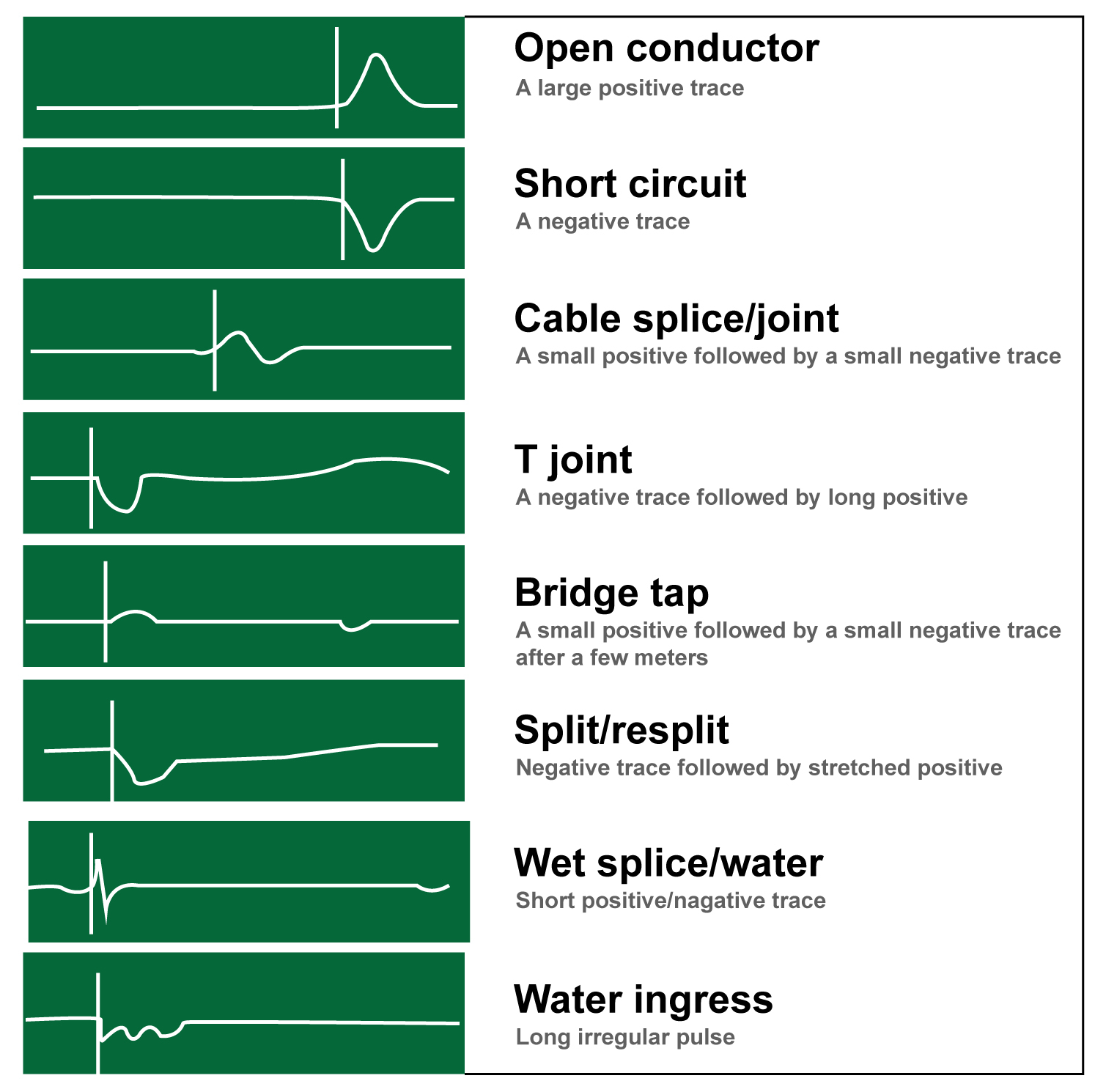
- Test traces: You can position test points on the traces that imitate the sensitive traces. These test points can be connected to oscilloscopes, TDRs, or signal generators to know the behavior of the signals. A test point can be placed in the auxiliary clock output for trigger or synchronization during testing.
- LED: You can incorporate LEDs in testing methods to determine whether the power is switched on or off. Debug LEDs are a suitable choice for FPGA or microcontrollers since they require debugging errors in the code.
- Selection of the test method: Choose the right method as per your design. The flying probe test is preferable for small production because of its simple setup and slow testing speed. The in-circuit test (ICT) involves fixed programming and is suitable for large production.
- Headers: These are a kind of test point connected to vias to measure the voltages across it.
- Additional circuit features: If the board has enough room, some circuitries are introduced to check the voltage and current of the components. These are non-essential yet helpful in validating the components’ rating.
What are the design for testing techniques?
Here are the two important testing techniques:
Bare board testing
Bare board testing is performed to check the PCB’s connectivity before assembling the components. Following are the two ways to perform this kind of testing:
- The isolation test verifies the resistance between two electrical connections.
- The continuity test checks if there is any presence of an open circuit within the board.
Assembled board testing
Assembled board testing is executed after assembling the components. This process ensures the circuit board’s integrity and the correct functionality of the components.
Here’s what Harry Kennedy, Electrical Engineer at Altair, has to say about optimizing your PCB designs for testing.
7 major DFT methods in PCB
1. Flying-probe test
The bare board and assembled board can both incorporate the flying probe test in passive and active mode, respectively. The probes comprise needles for checking. The test points can include passive components like resistors, capacitors, inductors, untented vias, or the terminating end of the components.
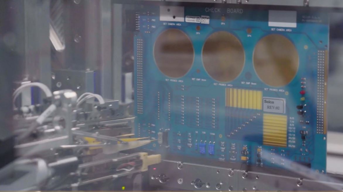
It can detect the value of non-powered elements, and open or short circuits, measure voltages, and check the placement of diodes, and transistors. Flying probe test is the most preferred choice over ICT in recent years.
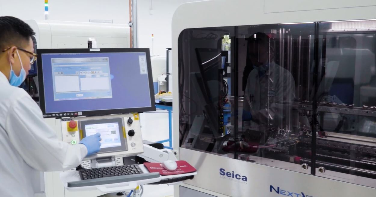
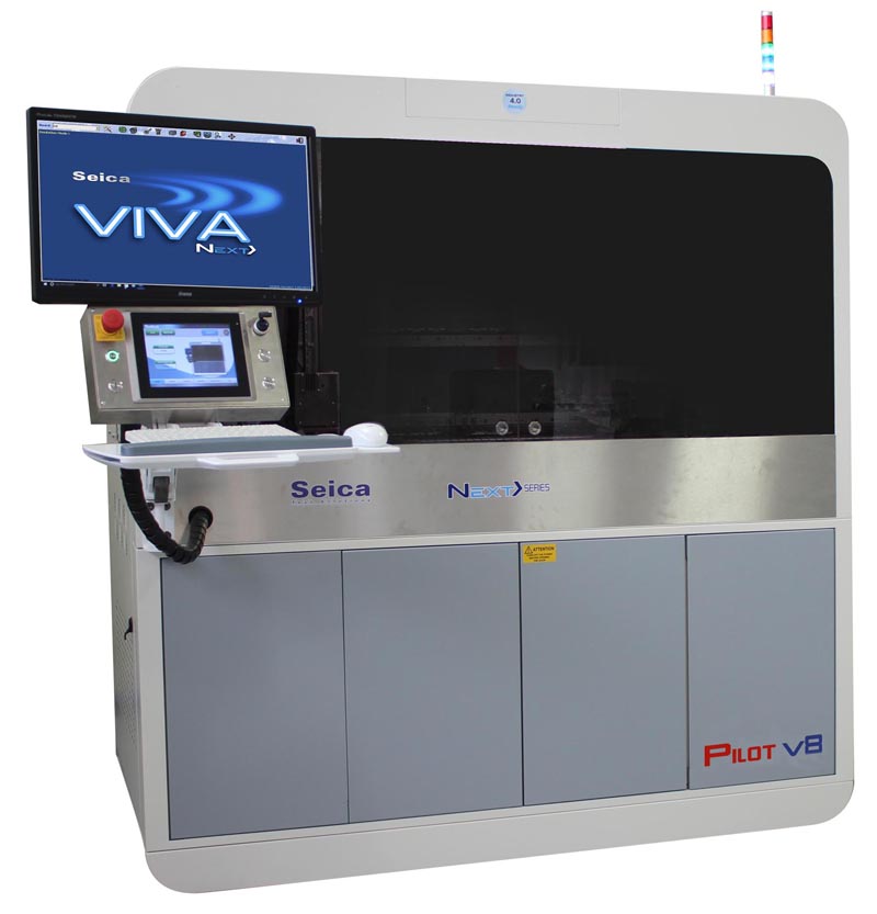
At Sierra Circuits, we use Seica Spa Pilot V8 for flying probe testing. This latest machine provides maximum performance, increased test speed, and low to medium volume run. Simultaneous vertical probing on both sides of the circuit board quickens the debugging process and enhances the flexibility for prototyping.
Guidelines for test point design and placement
(source: DFT (Design for Testability) for SEICA systems)
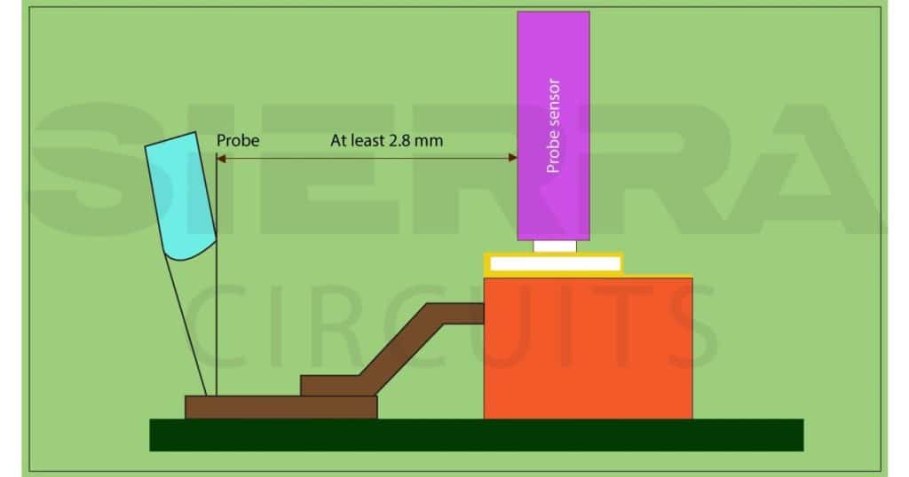
Accessibility to nets
- Nets linked to the active components must be accessible on the same side of the test probes. This leads to enabling the “openfix” option. Apply the same rule for SMD components as well
- For better efficacy, maintain a distance of 2.8 mm between the probe and the probe sensor
- This condition does not apply to the vertical testing procedure and to the board that is to be tested on both sides
Features of test points
- Preferrable contact points of the FPT process are:
- Test pads without solder resist
- Vias
- Through-holes
- PTH and SMD component pads
- Size of a test point:
- Dimensions depend on the probe type
- The minimum size is 6 mil (20 mil recommended)
- The spacing between one test point to another should be a minimum of 10 mil and
20 mil
- Vias:
- The diameter should be between 8 to 20 mil (10 mil recommended)
- Vias must be occluded and free from the solder resist
- For SMD components, particularly with steps slower than 25 mil, apply a solder pad that is longer than the component pin. This enables the testing probe to contact the test point not on the pin but on the soldering pad itself
- For horizontal architecture (PILOT L4/H4), components should be 4 to 5 cm higher than the
opposite of the test side
Board clamping
- The board is secured with a clamp/conveyed via, either horizontally (Pilot L4) or vertically (Pilot V8)
- For testers with horizontal architecture, provide support after every 150 mm or the distance based on your design requirement on both axes (except the Aerial and V8 test systems) to keep the board flat
Board dimensions
- Maximum board dimensions of 600 x 1010 mm for Pilot L4 testers
- Maximum board dimensions of 600 x 540 mm for Pilot V8 testers
Maximum component height
- CAD data must include the component height
- Component height calculations for horizontal Pilot L4 testers:
- Maximum board height + components on the head side: 40 mm, including the
board width - Maximum board height + components on the bottom side: 100 mm
- Maximum board height + components on the head side: 40 mm, including the
- Component height calculations for vertical Pilot V8 testers:
- Maximum board height + components on either side: 40 mm, including the board
width
- Maximum board height + components on either side: 40 mm, including the board
- The design team provides a list of components whose height is over 17 mm
Test point distances
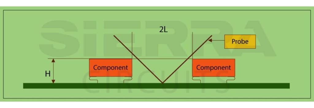
- The clearance is the distance between the center of the test point and the side of the component
- The minimum distance between a test point and the component can be estimated
by the formula:
L = (0.29 x Height) + 0.7 (in mm)
E.g. For height H= 4 mm, L= (0.29 x 4)+ 0.7 = 1.86 mm
- GND access is provided preferably at the 4 angles of the board
Fiducial recognition
- Include 3 fiducials for each board
- Position the fiducials in a triangle shape on either side of the board. It is essential to achieve different arrangements of the fiducials to eliminate side errors
- For the larger boards with dimensions greater than 400 mm, place local fiducials concerning the fine-pitch components which must be visible after the component has been mounted
Wire connection
- Wiring should be refrained from colliding with the test points.
Option for openfix
- To avail openfix, nets to be tested and connected to the active components must be accessible on the same side of the testing probe. This is also applicable to SMD connectors
- For better results, maintain a distance of 2.8 mm between the probe and the probe sensor
Benefits
- Less expensive.
- Greater test coverage.
- Do not require a fixture.
- Quick implementation.
Drawbacks
- Time-consuming since probes move between measurement points.
- Tough to set up if the board does not include any test point, test via, or masked via.
- The lump-sum capacitance can only be tested for the capacitors in parallel.
What FPT can check
- Performance of the components
- Flaws in assembly
- Open traces
- Short connections
- Misplacement of components
- Value of capacitance, resistance, and inductance

Design for Testing Handbook
7 Chapters - 28 Pages - 45 Minute ReadWhat's Inside:
- PCB testing strategies
- Guidelines to design and place a test point for FPT
- Directives to make your board ICT compatible
- Benefits and drawbacks of various testing methods
- Defects that you can identify through board testing
Download Now
2. In-circuit testing
The in-circuit test is also known as the bed of nails testing method. This process incorporates some pre-mounted, electrical probes aligned under the board through the preset access points. The accurate, and stable electrical connection between the probes and the PCB can be established in this way. The testing probes can cause to flow current on the pre-determined design test points.
ICT can check for shorts or open circuits, solder mask shortcomings, misplacement or absence of components, etc. This method comprises testing fixtures to hold the board with the probes correctly, and test jigs to check multiple components on a board simultaneously. This test method saves time.
Directives to achieve perfect ICT
(Source: DFT Design for Testability) for SEICA systems)
Accessibility to nets
As a general rule, all the nets must be accessible on the same side to the measuring heads, preferably the flip side, comprising the maximum number of components. A limited number of access points is permissible on the opposite side to eliminate the hindrance of accessibility to test pads and to increase the test coverage. This principle is not applicable to Aerial or V8 test systems.
Accessibility to NC nets (no connect) or Not used
- The NC nets, which are fill-in pins, need not be accessible
- The “Unused” nets, which are functional pins, will have accessibility, except for the Jtag nets (short-circuit detection)
- All the connector pins should be accessible
Access choice
Following priority order is to be maintained while accessing the nets:
- Test points
- Connection points: Through-hole components, connectors
- Vias
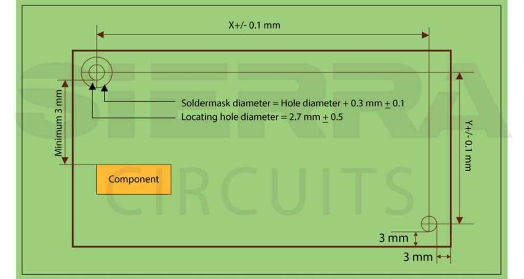
Board clamping or locating points
Depending on the board size, two or three locating points are required:
- At least 2 in the bigger diagonal
- 3, if the board side is greater than 400 mm
- More than 3 for the larger board
- Include 2 locating points for each rigid part of the flex-rigid boards
Definition of holes
- Preferrable hole diameter is 2.7 mm with ±0.05 tolerance
- Hole locating tolerance is ±0.1 mm
- The solder mask blank is 0.3 mm around the locating holes
- Minimum clearance area:
- 3 mm between the locating holes and the board edge
- 3 mm between the edge of the locating holes and each physical element of the board, including the external copper nets
- The locating holes will not be metalized and shall never be used for other purposes
Test point minimum dimensions
| Test point diameter | Reliability | |
|---|---|---|
| 1 mm | Highest | |
| Minimum value recommended for TOP side (component side) | 0.9 mm | ↓ |
| Minimum value recommended for BOTTOM side | 0.7 mm | ↓ |
| By default for BOTTOM side (Prohibited on the TOP side) | 0.6 mm | Lowest |
Minimum test point size according to board dimensions
| Board length and width in mm | <75 | 75-150 | 150-300 | >300 |
|---|---|---|---|---|
| Recommended test pad diameter | 0.7 mm | 0.7 mm | 0.7 mm | 0.9 mm |
| Minimum accepted test pad diameter | 0.6 mm | 0.6 mm | 0.6 mm | 0.7 mm |
Solder mask and test point
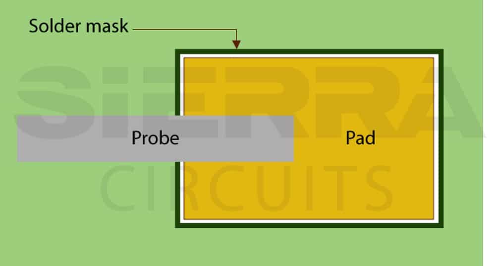
There must not be a solder mask on the test point. The solder mask can not be placed tangent to the test point.
Distance between the test points
The distance between the interaxis test points decides the kind of nail used to manufacture the test fixture. There are three types of nails, with different kinds of heads according to the contacts required: point, tulip, and diamond.
Nail choice
The choice of nails determines the cost and reliability. Nails of 1.27 mm diameter are used nails when all other possibilities can not be executed
| Nail | Cost factor | Reliability |
|---|---|---|
| 2.54 mm (100 mil) | 1 | Highest |
| 1.905 mm (75 mil) | 2 | ↓ |
| 1.27 mm (50 mil) | 4 | Lowest |
Minimum interaxis
| Minimum interaxis | Type of nail | |
|---|---|---|
| Minimum recommended value | 2.1 mm | 2.54 mm |
| Minimum recommended value | 1.7 mm | 1.905 mm |
| TOP side prohibited by default | 1.25 mm | 1.27 mm |
Distance between the test point and the component edge
| Component type | Distance |
|---|---|
| Height < 2 mm | 0.7 mm |
| Height > 4 mm | 1.91 mm |
| Board edge | 0.9 mm |
| Hole edge | 0.9 mm |
| Locating edge | 3 mm |
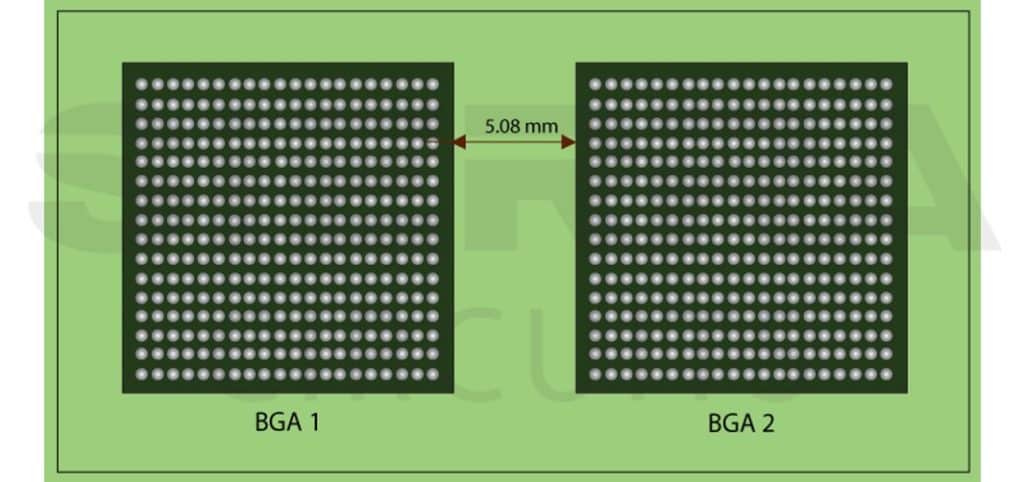
Test point under a BGA component
With a significant amount of pressure exerted by the nails under BGA components, there is a high risk of breaking the solder joints. Hence, it is crucial to avoid placing a test point under a BGA component. At least, leave a 5.08 mm (200 mil) gap on the four sides of the BGA to allow the placement of the upper contrast with a 3 mm diameter. This clearance is common if two BGA components are placed side by side.
Test point density
Distribute the test points on the entire surface to mitigate distortions and mechanic warpage. The test point density should be lower on the board edge with respect to the average board density.
Precautions
Check and ensure that the access to the test points is not covered by a connector or by mechanical parts mounted after manufacturing and before the in-circuit test.
Accuracy measurement
Incorporate a doubled test point on either side of the component or 4-wire measurement for the components such as resistors below 100 Ohms and capacitors with an accuracy of 0.1% or with lower functional value.
Access to the board power supply
For each power supply, 4 test points are scheduled to supply a current lower than 1 A. An additional test point can be added to give a rise of 0.5 A in the current. It is feasible to schedule as many test points as possible according to the powers on the connector of the board.
Wire rework
It is significant to keep in mind that while executing wire rework test points must be excluded from any kind of wiring connection.
Benefits
- Used for large production volume.
- Provides coverage up to 90%.
- Accurate. Free from human error.
Drawbacks
- Not suitable for small volume production.
- Voids or inadequate solder masks can not be detected.
- Expensive. Technologies like test jig add to more costs.
What ICT can check
- Incorrectly inserted component
- Wrong component
- Improper orientation of diodes, transistors or ICs
- Short circuits and open circuits
3. Functional testing
It is implemented for quality control and ensures the intended operation of a device. The test parameters are provided by the customers/designers depending on the design. The technique often incorporates simple switch on/switch off tests, and sometimes it requires complex software and precise protocols. Functional testing directly checks the board’s function in real environmental conditions.
Benefits
- Low cost.
- Versatile and can be customized as per the design.
- Doesn’t impact the lifespan of the board, unlike other tests that exert excessive stress on it.
Drawbacks
- Requires experienced technicians.
What FCT can check
- Checks the entire assembly
- Verifies boards’ functions in different working conditions
4. Automated optical inspection
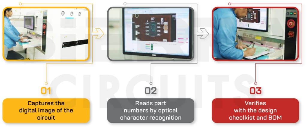
AOI incorporates 2D or 3D cameras that click high-resolution images and verify the schematics. It also compares with the perfect and imperfect designs available in the database. This method can find all the visible errors with great accuracy. AOI is used with another type of testing method to ensure the correct results, for instance, AOI with the flying probe and AOI with the in-circuit test. It can be included directly on the production line to prevent any premature board failure.
How AOI works
- Capture images: Automated optical inspection incorporates an advanced, expensive camera. These cameras range from extended graphics array (XGA) to multi-megapixel high-resolution sensors. After component placement and soldering, the board is passed through the AOI device. The camera captures multiple images. Successful assembly creates a golden standard. In the subsequent production runs, AOI scans and compares new images with the existing golden standard.
-
- Optical system resolution or imaging resolution is critical. It determines the extent of the details visible to the AOI. The resolution is influenced by inspection speed, accuracy, and size of the smallest component used on the circuit board. The camera’s sensor, lens, and the distance from the board are also key factors in determining imaging resolution.
- Field of view (FOV) is defined by the resolution of the camera sensor. It is the area of the board that can be covered by a single image.

- Proper illumination for visual inspection: It is paramount to scan and inspect various parts. Different kinds of lights such as incandescent, fluorescent, infrared (IR), and ultraviolet (UV) are involved in AOI. New technologies incorporate LEDs as the light source to procure an even and consistent form of lighting. The lighting system consists of red, white, green, and blue LEDs in a configurable lighting module. These LEDs provide an even and consistent form of lighting.
Benefits
- Fatal defects can be detected with accuracy.
- Consistent approach.
Drawbacks
- Only surface defects can be detected.
- Time-consuming process.
- Setups are subjected to change based on design.
- Detection based on the database is not always 100% accurate.
What AOI can check
- Lifted and misplaced component
- Open circuits
- Solder shorts
- Insufficient or excess solder
5. Burn-in testing
The burn-in testing is an early check-up of the board to prevent dangerous failures after fabrication is done. This method involves exceeding the specified operating limits to trigger the failures. This is an efficient way to detect the maximum operational rating of the board.
The various operating conditions involve voltage, current, temperature, operating frequency, power, and other factors pertinent to the design.
Benefits
- Increases product reliability.
- Verifies the functionality of the board concerning the ambient conditions.
Drawbacks
- The exerted stress beyond the rating can reduce the board’s lifespan.
- The process involves more time as well as more effort.
What burn-in test can check
- Examines the reliability of the specified parameters of the components
6. X-ray inspection
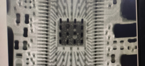
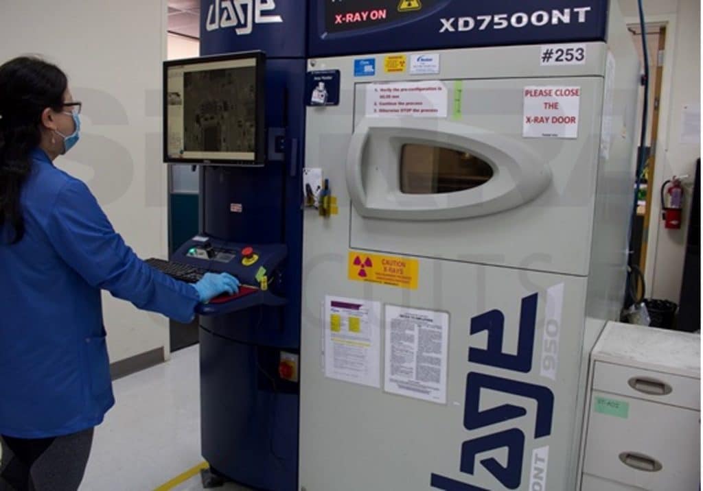
X-ray inspection detects errors in the hidden components, solder connections, BGA packages, internal traces, and barrel with the help of X-ray imaging.
AXI process flow
- The PCB, under test, is exposed to the X-ray radiation generated by a tube.
- A detector can capture X-rays passing through the sample board and transform them into a visual representation. Generally, heavy materials absorb more radiation than lighter ones. On X-ray scanned images, heavy materials appear darker, whereas lighter materials are more translucent to the radiation. In the case of PCBA, solder joints are made of heavy materials, and other parts, such as packages, silicon ICs, and component leads, are made of light materials. Hence, high-quality solder joints look darker in images than other parts.
- X-ray inspection systems should have enough magnification to ensure the correct information during defect analysis.
Benefits
- It is not required to check each layer of the PCB. An X-ray machine can easily check the internal layers from the top of the circuit.
Drawbacks
- This requires experienced and skilled technicians.
- The process demands more labor and cost.
What AXI can check
- Misalignment of components
- Solder void
- Solder quality
- BGA open and short connections
7. Visual inspection
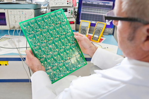
Here a technician inspects with bare eyes or by using a magnifier. This method can determine the unveiled components’ alignment, absence of components, and other defects.
Benefits
- Easy and basic method.
Drawbacks
- Subjected to human errors.
- Minor and invisible defects can not be detected.
What visual inspection can check
- Missing component
- Contaminated solder paste
- Solder joint reflow
- Warpage issues
PCB testing strategy
Width of border edge
This is essential to keep sufficient, unoccupied space along the opposite edges of the board. These clear edges are helpful to hold the testing machine perfectly. Generally, the standard width of the unavailable edges is maintained at 3 mm. Often, panel wastes are also incorporated for the same purpose.
Fiducials
The machine needs some reference points to know the exact position of the probes. The reference points, known as fiducials, are located on the panel waste, and on the PCB itself, if the waste has been removed. The most suitable and recommended fiducials are top-left and bottom right of the board.
Vias
The vias incorporated in the board design need to be non-masked to position a probe on the edge of them.
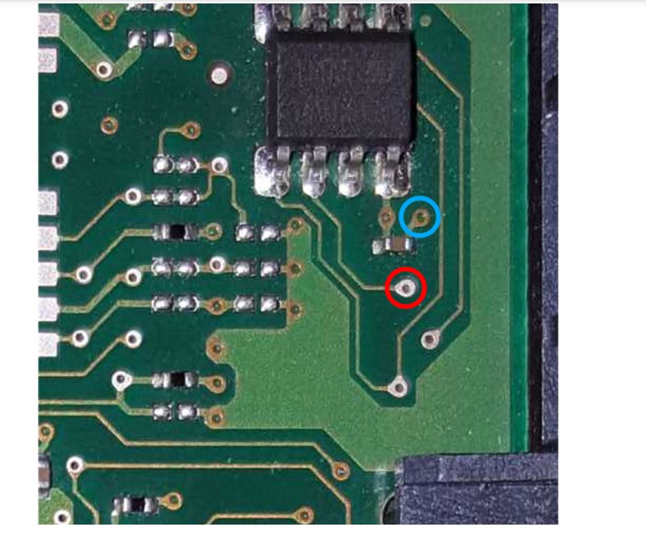
Component legs
Often, it is better to place the test probe near the component legs to achieve a good solder joint, though the component legs need not be tested. This technique connects any potential open circuit at the point of the test by pushing the component leg onto the pad.
Size
Place the test access points as close together as possible if you design a large board.
Cleaning
Cleaning the assembly is crucial to ensure the removal of unwanted flux. It is because sometimes the tester has to move the probe position to get better contact, undesired flux can cause failure and increase the test time.
Probe points
You can introduce accessible probe points in the ground and power rails on the bottom, perhaps on the unprobed side of the PCB. This allows fixed probes to act as temporary fixtures that speed up short testing and can reduce the overall test time and cost.
Test access
It would be great if you can maximize test access on one side of the assembly if possible, at least have one probable point for each network. If you are using a double-sided machine, the cost increases to turn the board over to test both sides.
Component height
There is a maximum component height allowed for both the probed and the unprobed region of the PCB, typically around 40 mm and 90 mm, respectively. The tall components are placed on the bottom side if it is unprobed or fitted after the test. They can create a no-fly zone on the assembly and also hinder test access.
Design for testing (DFT) is fundamentally a reviewing process to find and fix any manufacturing error, check the customer-provided specifications, and minimize excess process. Without this periodic testing, PCB manufacturers can face serious production errors. Assured DFT/DFA/DFM checks are one of the many benefits of choosing turnkey PCB manufacturing and assembly from a single fab shop. DFT ensures fabricating a board with a high yield at the minimum cost. If you’ve any queries regarding the design for testing, please comment below. We’ll gladly help you!
Check out our design guide to understand how design for manufacturability works.

Design for Manufacturing Handbook
10 Chapters - 40 Pages - 45 Minute ReadWhat's Inside:
- Annular rings: avoid drill breakouts
- Vias: optimize your design
- Trace width and space: follow the best practices
- Solder mask and silkscreen: get the must-knows


