Contents

On-demand webinar
How Good is My Shield? An Introduction to Transfer Impedance and Shielding Effectiveness
by Karen Burnham
System noise has become a critical issue for both analog and digital devices. The requirement for speedy interfaces and lower power consumption has resulted in devices being sensitive to disturbances from power and signal lines. A decoupling capacitor or bypass capacitor in a circuit provides high transient currents to an IC and reduces power ripples. Such capacitors are placed close to the power pins of an IC.
Analog circuits, such as audio amplifiers, produce a hum or a crackling noise during operation, while digital circuits, like microcontrollers, exhibit erratic and unpredictable behavior. It happens because the input voltage is not stable.
Any device will perform accurately if variations such as glitches, voltage spikes, and AC components remain within the tolerance. A good PCB design must ensure smooth input voltage by addressing intra-system power noise with adequately placed decoupling and bypass capacitors.
Why is decoupling necessary?
Decoupling provides a low-impedance path from the power supply to the ground. Therefore, choosing a low-inductance but high-value capacitor (low impedance) is very important.
Controlled Impedance Design Guide
6 Chapters - 56 Pages - 60 Minute ReadWhat's Inside:
- Understanding why controlled impedance is necessary
- Stack-up design guidelines
- How to design for impedance
- Common mistakes to avoid
Download Now
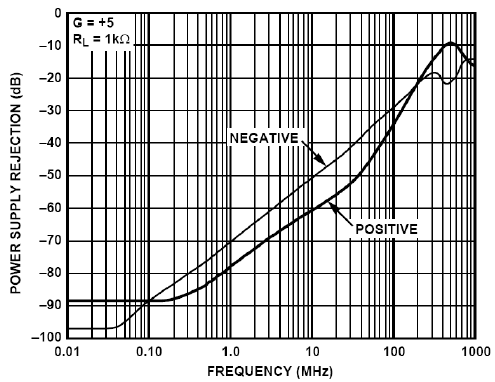
The graph given below depicts both positive and negative power supplies. It shows how the power supply rejection (PSR) of a high-performance amplifier deteriorates with a frequency of around 20 dB/decade.
Around 90 dB at DC, the PSR drops rapidly at higher frequencies, which signifies coupling of unwanted energy on the power line to the output.
That’s why it is obligatory to avoid this high-frequency energy from entering the IC. It can be done by incorporating electrolytic capacitors (for low-frequency decoupling) and ceramic capacitors (for high-frequency decoupling).
Power supply rejection specifications are not necessarily specified in the datasheets. But you can always find the recommended power supply decoupling circuits in the applications section of the datasheet. These recommendations should always be followed customarily to ensure the proper operation of the device.
Sensitivity of an IC
The sensitivity of an IC to power supply fluctuations is represented by the power supply rejection ratio (PSRR) or PSR (in dB). PSRR is the ratio of the change in output voltage to the change in power supply voltage.
What is a decoupling capacitor?
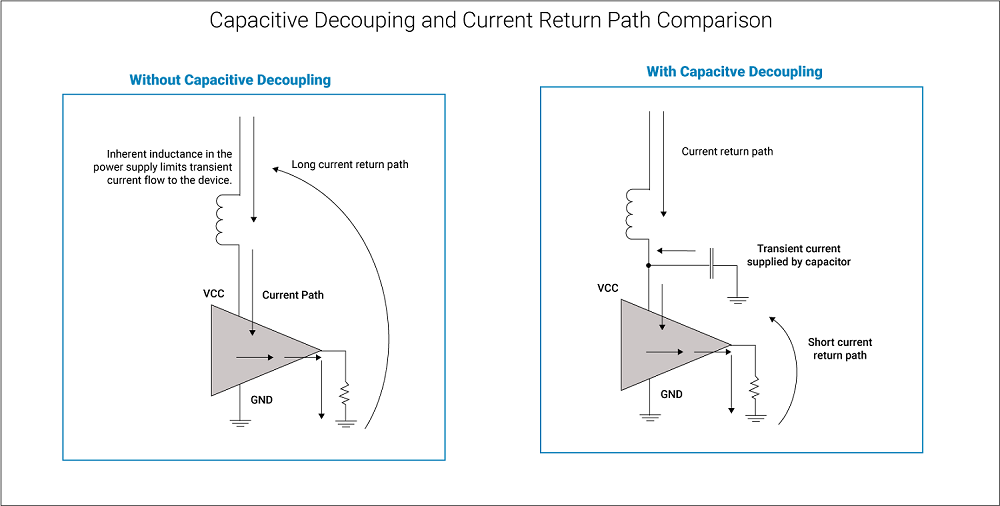
A decoupling capacitor is a passive component capable of storing energy in a localized manner. Because of its very nature, it takes time to charge and discharge. It prevents quick changes in the voltage, protecting the system or IC by providing a proper DC supply.
The decoupling capacitor is connected in between the power supply and load/IC in parallel. To inhibit the voltage disturbances for each IC, they must be placed locally, i.e., as close as possible to the IC.
All power distribution networks have actual impedance and inductance that prevent the instantaneous supply of current; the capacitor controls voltage supply dips and ringing and ensures stability in the circuit voltage.
What is a bypass capacitor?

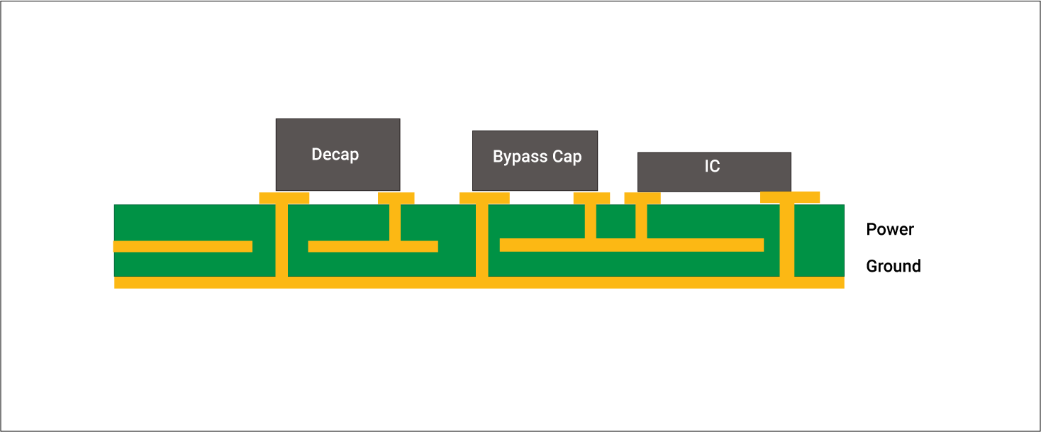
A bypass capacitor prevents noise from entering the system by bypassing it to the ground. It is connected between the supply voltage (Vcc) and ground (GND) pins to reduce power supply noise and voltage spikes on the supply lines.
What is the difference between decoupling and bypass capacitors?
The decoupling capacitor stores energy and dissipates it back into the power rail to maintain the smooth flow of current. The bypass capacitor provides the AC signal return path to switch between the power and ground rail.

Considering their purpose and function, both bypass and decoupling capacitors can be used interchangeably. When powering any device, the primary objective is to provide a very low impedance path with respect to the input power ground. Some of the few noticeable differences are:
- Bypass capacitors provide a low-impedance shunt path to the high-frequency noise signals. They ensure high-frequency noise is mitigated before it flows into the entire circuit, resulting in circuit malfunction and an EMI problem. On the other hand, decoupling capacitors stabilize the voltage variations.
- For low-impedance shunting, a single electrolytic capacitor is sufficient, but for stabilizing the signal, two different types of capacitors are required.
See how to handle current return path for better signal integrity.

High-Speed PCB Design Guide
8 Chapters - 115 Pages - 150 Minute ReadWhat's Inside:
- Explanations of signal integrity issues
- Understanding transmission lines and controlled impedance
- Selection process of high-speed PCB materials
- High-speed layout guidelines
Download Now
What is the purpose of a decoupling capacitor?
Decoupling capacitors are used to isolate or decouple two circuits. In other words, they decouple AC signals from DC signals or vice versa.
- In case of input voltage drop, it provides adequate power to an IC to maintain the voltage level.
- In case of a voltage surge, a decoupling capacitor prevents the excess current from flowing through the IC to keep the voltage stable.
What type of capacitors are used for decoupling?
Power supply circuits incorporate different types of capacitors, such as electrolytic, tantalum, and large-value capacitors. The primary purpose of a decoupling capacitor is to establish a low-impedance path.
We know the resonant frequency of a capacitor, f = 1 / (2π × √(L × C))
Where,
f: resonant frequency;
L: circuit inductance; and
C: circuit capacitance.
Atar Mittal, General Manager at Sierra Circuits, says, “Below the resonant frequency, the capacitor functions as a typical capacitor, but beyond it, it starts behaving like an inductor. Electrolytic and tantalum capacitors are typically associated with low-frequency applications, while ceramic capacitors are versatile and can operate across mid and high-frequency ranges.”
In this section, you will learn the features of different capacitors used in circuit design.
Electrolytic capacitors
Larger electrolytic capacitors (1 to 100 μF) are used to decouple low-frequency noise. These capacitors act as charge reservoirs to fulfill the instantaneous charge requirements of the circuit. Such capacitors should not be placed more than 2 inches away from the IC.
Since all electrolytic capacitors are polarized, they cannot withstand more than 1 volt of reverse bias without damage. They have relatively high leakage currents, which depend upon the design, electrical size, and voltage rating vs. applied voltage. Nonetheless, leakage current does not significantly affect decoupling.
Ceramic capacitors
Low inductance surface-mount ceramic capacitors are used to decouple high-frequency power supply noise. These capacitors are connected directly to the power supply pins of the IC.
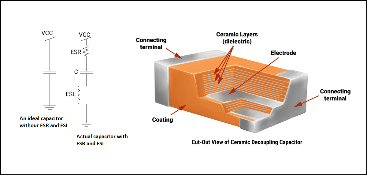
Ceramic capacitors with capacitances of 0.1 or 0.01 μF possess high resonant frequencies, making them capable of filtering out high-frequency noise. This is why low-value ceramic capacitors are employed to attenuate high-frequency noise in the power distribution network.
Ceramic capacitors are compact and have a low loss. They have wide temperature tolerance, low ESR/ESL, stability, and reliability, and can withstand wide voltage ranges. X7R, Z5U, and Y5V capacitor types are available in values up to several μF with high dielectric constant and voltage ratings up to 200 V.
The X7R-type ceramic capacitor is preferred because it shows less change in capacitance as a function of DC bias voltage compared to Z5U and Y5U.
Additionally, NP0 (COG) ceramic capacitors (0.1 μF or less) are also used because of their lower dielectric constant formulation and low voltage coefficient.
Multilayer ceramic (MLCC) surface-mount capacitors
MLCCs are used for bypassing and filtering at 10MHz or more because of their low inductance design.
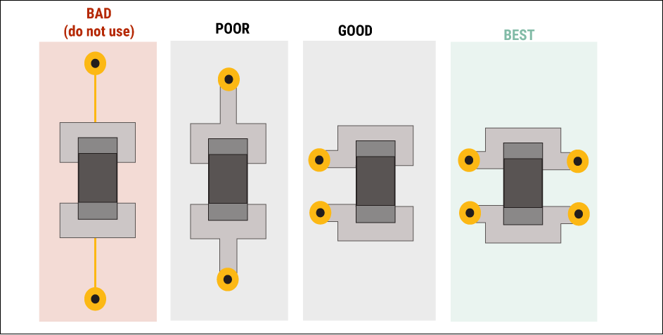
In order to be more effective, all decoupling capacitors must be connected directly to a low impedance ground plane. It is advisable to connect these capacitors using short traces or vias to minimize the series inductance.
How do you place a decoupling capacitor?
The placement of the decoupling capacitor is crucial because it reduces the impedance of power supply rails. Ideally, it should maximize the capacitance and minimize the resistance and inductance. Components like ICs depend on their input voltage to be as steady as possible while operating.
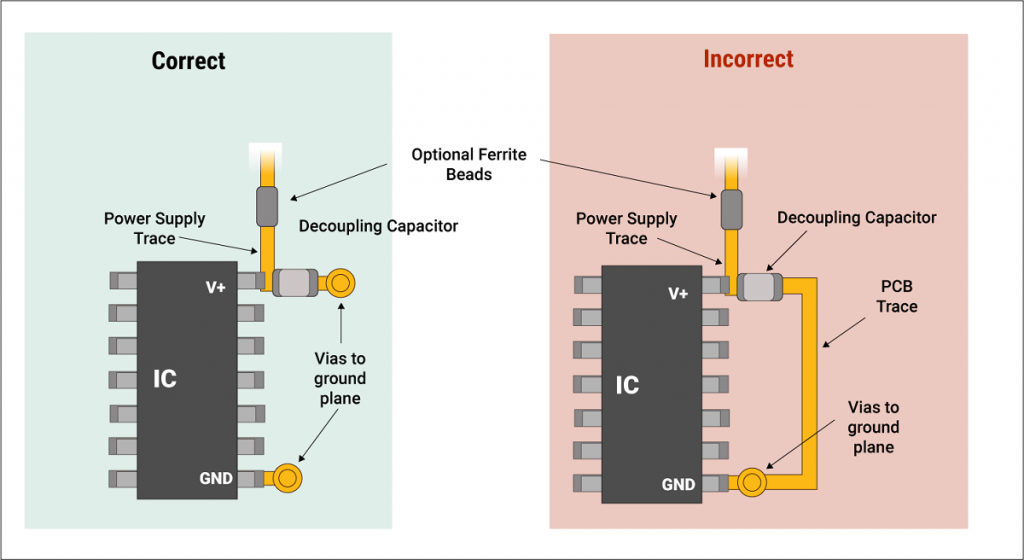
- It should be placed as close as possible to an IC because it protects these sensitive chips by filtering out any excessive noise. The farther away they are, the less effective they will be.

In the figure on the left (as shown above), the connection to both the power pin and the ground is made as short as possible. It is the most effective arrangement. In the figure on the right (as shown above), the PCB trace may cause interference issues by forming a loop. This arrangement is less effective because of the excess inductance and resistance of the PCB trace.
- Always connect decoupling capacitors between the power source and load/IC in parallel to one another.
- Placing a capacitor in series with input and output signal traces removes low-frequency transients from the input and output signals.
- Placing a capacitor in parallel with a resistor reduces high-frequency EMI.
- When using vias to reach the power plane, connect the capacitor to the component pin, then to the via to ensure current flows through the plane.
- Decoupling capacitors are also effective for isolating analog and digital signals. It is achieved by connecting a capacitor between AC and digital PCB ground pours.
- Make sure that power and ground planes are continuous and adjacent: Placing capacitors close to the power and ground pins of ICs is crucial. It makes circuit paths to ground and power planes as short as possible.
- The symmetrical placement of adjacent power and ground planes: Adjacent power and ground planes should be placed symmetrically. It is also advised to minimize the number of layers between the planes and the decoupling capacitors.
For more information, read our blog on Decoupling capacitor placement guidelines for PCB design.
How do you choose the value of a decoupling capacitor?
The number of capacitors to be used in a circuit depends on the number of power and ground pins and I/O signals present. Choose decoupling capacitors with sufficiently high self-resonant frequencies based on the signal bandwidth or operating frequency.
Understand the self-resonant frequency: The capacitor remains capacitive up to this frequency and starts to appear as an inductor above this frequency. The impedance of a decoupling capacitor reaches the minimum impedance at the frequency ω =1 / √LC. This frequency is known as the resonant frequency of a decoupling capacitor.

Lower capacitance and lower inductance yield higher resonant frequency. A higher self-resonant frequency is achieved by selecting a smaller surface-mount component because, typically, a smaller component package has lower parasitic inductance.
The low-frequency noise decoupling capacitor value should lie between 1 µF to 100 µF. The high-frequency noise should lie between 0.01 µF and 0.1 µF.
- Low equivalent series resistance (ESR) and equivalent series inductance (ESL): Since a capacitor needs to provide current quickly, choose a capacitor with low ESR and ESL. Low ESR and low ESL indicate minimal internal resistance and inductance in capacitors and inductors. The datasheet for each component specifies this.
- Smaller package size: This is because smaller package sizes have lower ESL. Additionally, wide geometry capacitors are better than standard ones due to lower inductance. Since capacitors often connect to the IC through PCB vias, typically located on the board’s backside, minimizing via inductance is important.
Pay attention to the via geometry and placement on the capacitor pads. Also, aim for the ESR of the decoupling capacitors to match the IC’s characteristic impedance. If the ESR is too low, it can increase the quality factor (Q) of the internal package resonance, potentially affecting signal integrity.
How do you choose the size of a decoupling capacitor for digital PDN?
The size of the decoupling capacitor is evaluated based on the impedance of the power distribution network (PDN) and the charge required by the switching IC. Evaluating accurate capacitor size and placing it correctly helps to reduce ripples and noise on the PDN.
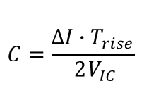
Calculate the decoupling capacitor size based on the current drawn during switching and IC voltage.
Where: Trise is the rise time, VIC is the IC voltage, and ΔI is the current drawn.
Note: The above formula is valid if the signal bandwidth is less than the self-resonance frequency of the decoupling capacitor. Signal bandwidth is given by: (0.35/signal rise time).
How do you choose the size of a decoupling capacitor for analog PDN?
When providing stable power for an analog IC, the decoupling capacitor constantly charges and discharges to provide stable power as an analog IC operates.
The size of the decoupling capacitor for an analog IC is given by:
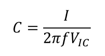
The current drawn by the IC would be an increasing function of the IC voltage and frequency.
Where f is the frequency, VIC is the IC voltage, and I is the current drawn.
How do you choose the size of a decoupling capacitor based on PDN impedance?
Decoupling capacitors provide the required charge in a timely manner and reduce the output impedance of the overall PDN. Practically, a it is only effective over a particular frequency range.
Its impedance decreases linearly with the decrease in frequency and increases with the increase in frequency. This increase in the impedance of a practical decoupling capacitor is due to the its parasitic inductance.
Also read, How to reduce parasitic capacitance in PCB layout.
One of the best ways to determine decoupling capacitor size is based on the target PDN impedance.
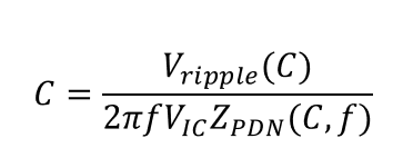
Its size is based on the required voltage ripple, target PDN impedance, and target PDN voltage.
Where f is the frequency, VIC is the IC voltage, Vripple is the voltage ripple, and ZPDN is the target PDN impedance.
Target PDN impedance and the PDN ripple voltage are functions of the capacitance, making it a very complex problem to solve. Calculating ‘C’ requires several iterations. The above equation is more accurate because it can incorporate the effect of the resonance frequency of the decoupling capacitor and resonances that arise due to parasitics in the PCB layout.
While calculating ZPDN for different values of C and f, we arrive at the best values of C to get the lowest ZPDN for all the frequency ranges.
Note: The exact value of the decoupling capacitors to be used is always provided with the ICs datasheet.
How do you choose the value of a bypass capacitor?
The reactance of the capacitor, added to the circuit, should match the difference in reactance between the transmission line and the driver. Current always takes the lowest resistance path, so if you want to switch the AC signal to the ground, the capacitor should have a lower resistance. The capacitance value of the bypass capacitor to be used is :

Where f is the frequency and XC is the reactance. ‘f’ depends on the operating frequency of the board.
X2Y capacitors are preferable for bypass/decoupling applications due to their lower ESL than standard 2-terminal capacitors. X2Y capacitors are 3-terminal devices with lower ESL and shorter electrical length from device end to the middle pad. This makes them more effective in reducing high-frequency noise. If you place X2Y capacitors on the bottom side of the board for an IC, you still have to account for via inductance. However, they require more board space than other capacitor configurations. An alternative is to use smaller capacitors placed end-to-end, which can mimic the performance of X2Y capacitors. Using wide geometry capacitors in this configuration can further reduce ESL.
Capacitors are one of the most versatile components used on PCB assemblies, and one of their most important functions is decoupling. Your board’s signal and power integrity may well depend on how effectively you place decoupling capacitors and bypass capacitors.






Start the discussion at sierraconnect.protoexpress.com