Contents

On-demand webinar
How Good is My Shield? An Introduction to Transfer Impedance and Shielding Effectiveness
by Karen Burnham
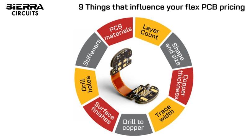
Cost optimization is one of the major objectives when designing a PCB. To achieve that, every designer should know the major cost drivers of a circuit board. The primary cost drivers of flex PCBs include board materials, layer count, efficient panel utilization, type of stiffeners, and surface finish.
9 flex PCB cost drivers
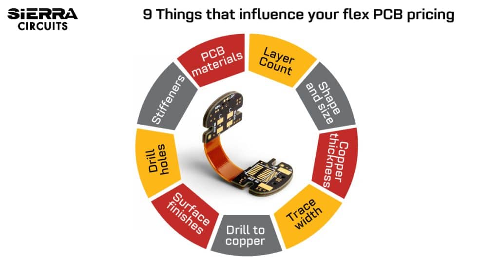
The overall cost of a circuit board mainly depends on the type of board (rigid or flex), materials used, the number of layers in the stack-up, and incorporation of HDI or ELIC (every layer interconnect) structure. Below are a few parameters that impact the overall price of a flex board:
1. Circuit board materials
The PCB material used to fabricate is one of the primary cost drivers of a flex board. Standard rigid boards are laminated using FR-4 substrates. Polyimide substrate is the most used material for manufacturing both flex core and coverlay layers.
Flex substrates offer better thermal and electrical properties when compared to standard FR4 laminates. The thickness of flex materials is uniform throughout the substrate. These substrates also offer improved Dk values ranging between 3.2 and 3.4. The lack of woven glass reinforcement reduces variations in Dk. Typically, the thickness of the flex layers ranges between 1 and 5 mils. Flex laminates may cost 2 to 3 times more than the standard rigid materials.
Read 9 cost drivers for rigid circuit boards.
Adhesiveless Vs. adhesive flex cores
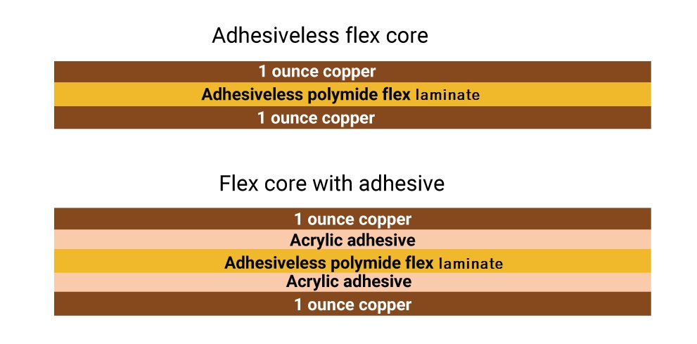
Adhesive-based flex cores use a flexible adhesive layer to attach each copper layer to the polyimide core under heat and pressure. The adhesive is commonly epoxy or acrylic-based and ranges in thickness from 0.0005″ to 0.001″. These materials are less expensive when compared to adhesiveless materials.
Copper is directly bonded to the polyimide core without using adhesives in adhesiveless flex cores. Though adhesiveless materials are expensive, they offer numerous advantages such as reduced flex thickness (due to absence of adhesive layer), improved temperature ratings, excellent plated hole reliability, and so on.
Factors that influence material selection for flex PCBs
- Thermal reliability: Always choose a material that meets the temperature expectation of the application. If the board is intended to operate in a high-temperature environment, the material should withstand high-intensity heat without transferring the heat to the adjacent components.
- Mechanical properties: This factor decides the material’s ability to withstand physical stress during its assembly or operation. Bend radius is one of the important physical parameters when it comes to flexible PCBs.
- Signal performance: It is the material’s ability to facilitate uninterrupted signal propagation throughout the operation cycle. This is critical in the high-speed and controlled impedance boards.
If cost is the primary concern, avoid over-specifying the material requirements. For example, consider polyester laminate over polyimide substrate if the application operates under a lower temperature environment. Simple flex boards (class 1 flex boards) can take the advantage of inexpensive lower temperature materials.
PCB Material Design Guide
9 Chapters - 30 Pages - 40 Minute ReadWhat's Inside:
- Basic properties of the dielectric material to be considered
- Signal loss in PCB substrates
- Copper foil selection
- Key considerations for choosing PCB materials
Download Now
2. Circuit layer count
The number of layers is another significant cost driver of a flex PCB. As the number of circuit layers increases, the overall cost of the board increases. The lamination process becomes complicated as more layers are added to the board. This will take longer and will demand a greater supply of materials. Processing issues that occur due to high layer count are:
- Layer-to-layer alignment
- Plated through-hole integrity
- Thermal expansion in the z-axis
- Lamination defects
Check our article on the importance of PCB layer count estimation to understand the significance of layer count and how it affects manufacturing cost.
The below table gives an estimate of the price increase as the layer count increases.
| Increase in layer count | Increase in overall cost |
|---|---|
| From 1 layer to 2 layers | 35 to 40% in comparison with a single-layer board |
| From 2 layers to 4 layers | 35 to 40% in comparison with a two-layer board |
| From 4 layers to 6 layers | 30 to 40% in comparison with a four-layer board |
| From 6 layers to 8 layers | 30 to 35% in comparison with a six-layer board |
| From 8 layers to 10 layers | 20 to 30% in comparison with an eight-layer board |
| From 10 layers to 12 layers | 20 to 30% in comparison with a ten-layer board |
3. Size and shape of the board
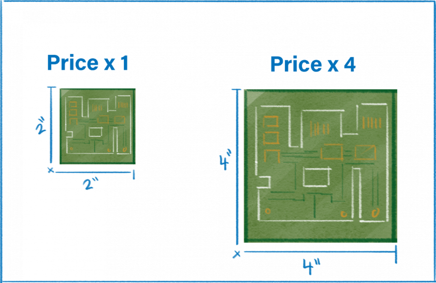
A circuit board’s shape and size (board outlines) are determined by a PCB designer. The larger the surface area, the higher the price. When multiple boards are fabricated within a panel, the panel’s surface should be efficiently utilized. Flex boards are fabricated in different shapes, such as squares, rectangles, circles, and many random shapes. Fabricating a random-shaped PCB may add to the cost as the panel utilization may come down.
4. Trace width and spacing
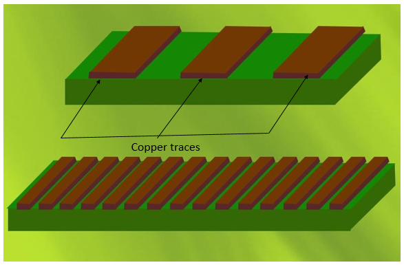
An appropriate trace width is required for signals to propagate through a trace without the risk of overheating. The tighter the spacing, the more difficult it will be to etch traces and pads reliably. This adds to the overall cost of the board.
5. Thickness of the copper foil
The cost of a circuit board increases as the thickness of the copper layers increases. When thick copper layers are implemented on the inner layers, more prepregs are required during lamination. These prepregs avoid resin starvation by filling the gaps between the copper sections. The PCB price rises when there is more than ½ oz of copper on the inner layers and more than 1oz of finished copper on the outside layer.
Another downside of using thicker copper is that significant spacing between traces must be maintained. Thicker copper will require a wider trace width. However, utilizing very thin copper (less than ¼ oz) will spike the costs due to extra processing costs.
6. Drill holes
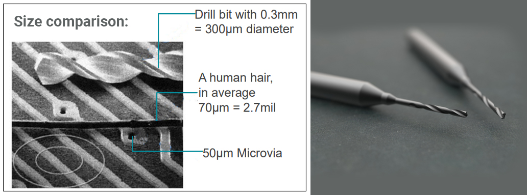
Size of the drilled holes
The standard drill bit is 8 mils in diameter, while the advanced drill bit is 5 mils. The smaller the drill hole size, the higher the duration of drilling. This results in higher overall costs.
To learn more about the PCB drilling process, read PCB drilling explained: The do’s and the dont’s.
7. Drill to copper
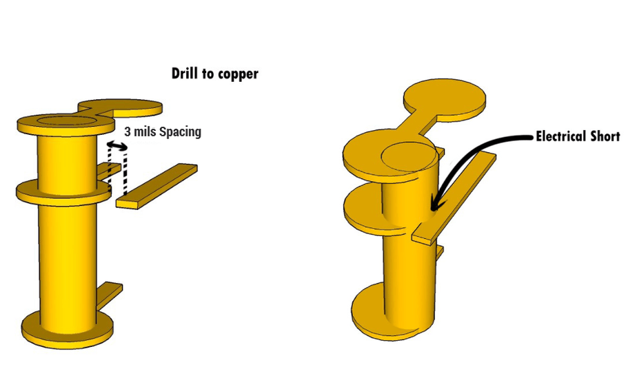
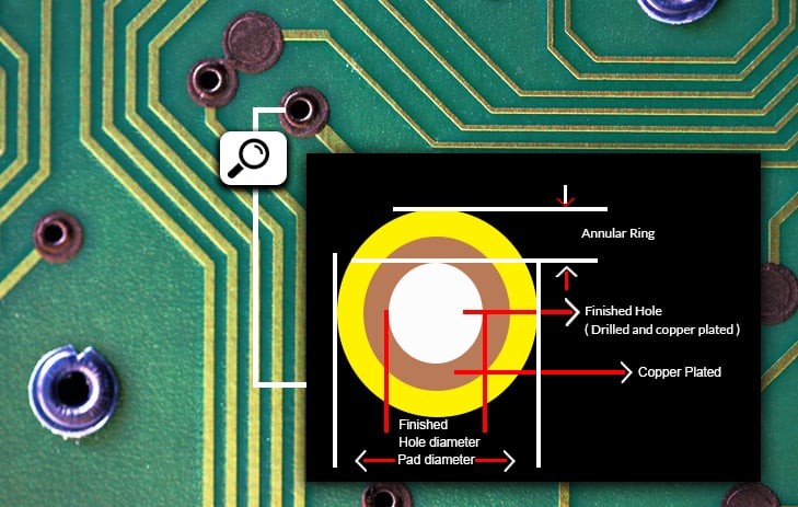
Drill to copper is the distance from the edge of the drilled hole to the nearest copper feature on a layer (pad, pour, and trace, etc.). Typically, drill to copper clearance is 8 mils. The smaller the drill to copper, the more expensive is the PCB manufacturing process.
To improve the manufacturability of these boards, refer to DFM for flex and rigid-flex PCBs utilizing SMT.
8. Surface finishes
A PCB surface finish is an intermetallic joint between the bare copper of the solderable area of the printed circuit board and the components. The surface finish should be chosen in a way that improves product performance keeping the cost in mind.
Types of PCB surface finishes
- ENIG (Electroless Nickel/ Immersion Gold): This is the most common type of circuit board surface finish. It’s popular because it doesn’t tarnish, it’s reliable. ENIG is more expensive than other surface finishes, but it offers superior PCB solderability. This surface finish sometimes results in the formation of black pad. This is where phosphorus accumulates between the nickel and gold layers. Fractures and incorrect board connections are the possible outcomes.
- Immersion silver: Silver is a robust finish material that may be used in a variety of applications. Because of its growing popularity, the material is becoming more freely available, lowering and stabilizing its price.
- Immersion tin: This finish involves depositing a thin layer of tin on a circuit board. Immersion tin provides a consistent finish. The disadvantage is that it has a short lifespan. However, it offers outstanding performance at an optimum cost.
9. Type of stiffeners
The overall cost of a flex PCB is also determined by the type of stiffeners employed. In a flex design, stiffeners serve the following objectives:
- Modification of thickness to meet ZIF connector specifications
- Component/connector area support
- Promote heat dissipation
FR4 and polyimide are the two most common stiffener materials. Although aluminum and stainless steel are employed in some designs, they are more expensive than FR4 and polyimide. Aluminum is a popular material for heat dissipation applications.
Stiffeners are bonded with either a thermally bonding adhesive or a pressure-sensitive adhesive (PSA). Thermal bonding adhesive is preferable, although design constraints may necessitate the use of a PSA. Thermal adhesives are flexible epoxy or acrylic adhesives that are used to attach coverlays to flex circuits, and they provide a permanent bond. They are less expensive than PSAs.
How to reduce the overall cost of flex and rigid-flex PCBs
1. Keep the number of layers as minimum as possible
The number of prepreg plies required is reduced as the number of layers in the design is reduced. Limiting the number of layers of flexible circuitry lowers the overall cost. Simultaneously, fewer layers boost the manufacturer’s ability to improve manufacturing yields.
2. Use rigid substrates to obtain overall thickness in rigid-flex designs
If a specific overall thickness needs to be attained, make use of rigid board laminates instead of no flow prepreg or flexible laminates. Flexible laminates are costlier than rigid laminates.
- Efficient panel utilization
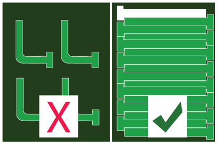
A panel, or a circuit board array, is a large sheet of material that contains several individual PCBs. Overall manufacturing costs can be reduced by efficient usage of panel surface area. The image above shows an example of inefficient and efficient flex panelization.
- Uniform stiffener thickness
Always use stiffeners with uniform thickness. This reduces the fabrication time and, in turn, reduces the cost.
To learn about the issues that increase the lead time of the flex board, see 5 factors that delay flex PCB quick turn delivery.
- Limit the number of vias
When compared to through-holes, blind and buried vias require significantly more manufacturing steps, which increase processing time and lower yields. Reducing the number of vias in the flex board can reduce the overall cost.
Cost optimization should be considered during the initial stage of circuit board design. Identifying the least expensive cost drivers of a flex PCB requires accurate design solutions and clear engineering strategies. Understanding the pros and cons of using a particular material, hole drilling techniques, stiffener types, trace width, spacing, etc., can help prevent future production failures. Planning ahead of time and having consistent discussions with your PCB manufacturer will help you optimize time and cost. Choosing turnkey PCB manufacturing and assembly from a single facility for your flex design has many benefits, like quality assurance and reduced turnaround.
Let us know in the comment section if you want to know more about our flex board capabilities.
Flex PCB Design Guide
10 Chapters - 39 Pages - 45 Minute ReadWhat's Inside:
- Calculating the bend radius
- Annular ring and via specifications
- Build your flex stack-up
- Controlled impedance for flex
- The fab and drawing requirements


