Speak to an Account Manager
![]() +1 (800) 763-7503
+1 (800) 763-7503
Related Categories — PCB Assembly
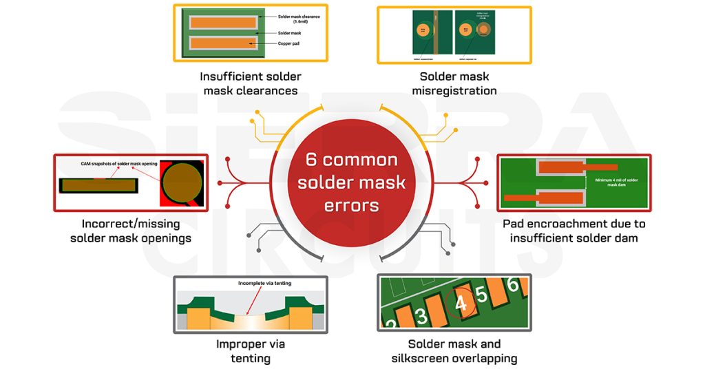
6 Common Solder Mask Errors Every PCB Designer Should Know
A solder mask is an insulation layer that covers conductive areas such as traces and pads. Inappropriate solder layer application […]
PCB Design
Case Study: Routing Microcontroller and BGA in Rigid-Flex PCBs
When routing microcontrollers and BGAs, you need to consider the trace spacing requirements of your design and clearance ... more »
Case Studies
Advantages of Ordering PCB Prototype and Bulk Production from a Single Fab House
Choosing the same fab house for PCB prototypes and bulk production has many advantages, such as better DFM ... more »
PCB Manufacturing
6 Common Solder Mask Errors Every PCB Designer Should Know
A solder mask is an insulation layer that covers conductive areas such as traces and pads. Inappropriate solder ... more »
PCB Design
Case Study: Routing Microcontroller and BGA in Rigid-Flex PCBs
When routing microcontrollers and BGAs, you need to consider the trace spacing requirements of your design and clearance ... more »
Case Studies
Advantages of Ordering PCB Prototype and Bulk Production from a Single Fab House
Choosing the same fab house for PCB prototypes and bulk production has many advantages, such as better DFM ... more »
PCB Manufacturing
How to Design and Build a Hybrid PCB Stackup
A hybrid stackup construction enhances your PCB’s performance and cost-effectiveness by combining different materials or technologies. It helps ... more »
PCB Manufacturing
Case Study: Eliminating BOM and Footprint Errors in PCB Assembly
Sticking to DFA benchmarks ensures components are correctly assembled on a PCB without any discrepancies. DFA brings down ... more »
Case Studies
Case Study: Designing 8 and 14-Layer HDI PCBs with Stacked Vias
Stacked vias are considered the most suitable solution for manufacturing HDI boards with advanced features. The configuration, with ... more »
Case Studies
How Sequential Lamination is Performed to Manufacture HDI PCBs
Sequential lamination is a process of fabricating a circuit board using subsets composed of copper and dielectric layers. ... more »
HDI / Blind & Buried Vias
Case Study: Designing an HDI Board with 0.4 and 0.65 mm BGAs
BGA technology makes it possible to achieve a smaller form factor in PCBs. With a higher pin count, ... more »
Case Studies
How to Optimize Your PCB Trace Using IPC-2152 Standard
IPC-2152 is the standard for determining the current capacity, temperature rise, and width of a trace in a ... more »
IPC


Fabrication, Procurement, & Assembly. PCBs fully assembled in as fast as 5 days.
- Bundled together in an entirely-online process
- Reviewed and tested by Engineers
- DFA & DFM Checks on every order
- Shipped from Silicon Valley in as fast as 5 days

Fabrication. Procurement & Assembly optional. Flexible and transparent for advanced creators.
- Rigid PCBs, built to IPC-6012 Class 2 Specs
- 2 mil (0.002″) trace / space
- DFM Checks on every order
- 24-hour turn-times available

Complex technology, with a dedicated CAM Engineer. Stack-up assistance included.
- Complex PCB requirements
- Mil-Spec & Class 3 with HDI Features
- Blind & Buried Vias
- Flex & Rigid-Flex boards