Speak to an Account Manager
![]() +1 (800) 763-7503
+1 (800) 763-7503
Related Categories — PCB Design » PCB Materials » Signal Integrity
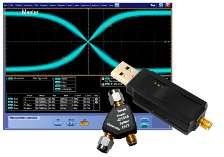
PerfectPulse Is the Pocket-Sized TDR Every Engineer Needs
For only $3,500, you can now own a precise portable TDR/TDT (Time Domain Reflectometer / Time Domain Transmissometer). It is compatible with sufficient bandwidth 50-ohm probes. Are you wondering where the name comes from? It is “because the pulse is close to perfect,” Steve Sandler, CEO of Picotest, told us.
PCB Manufacturing
Signal Integrity: Via Stubs and Their Effects on Signal Attenuation and Data Transfer Rates
First, let's start with a few things to know about signal integrity and via stubs. A via stub ... more »
PCB Design
How to Reduce EMI to Improve Signal Integrity
EMI may be caused by unexpected radiated emissions as well as though interference conducted along cables and traces. ... more »
EMI and EMC
PerfectPulse Is the Pocket-Sized TDR Every Engineer Needs
For only $3,500, you can now own a precise portable TDR/TDT (Time Domain Reflectometer / Time Domain Transmissometer). ... more »
PCB Manufacturing
Signal Integrity: Via Stubs and Their Effects on Signal Attenuation and Data Transfer Rates
First, let's start with a few things to know about signal integrity and via stubs. A via stub ... more »
PCB Design
How to Reduce EMI to Improve Signal Integrity
EMI may be caused by unexpected radiated emissions as well as though interference conducted along cables and traces. ... more »
EMI and EMC


Fabrication, Procurement, & Assembly. PCBs fully assembled in as fast as 5 days.
- Bundled together in an entirely-online process
- Reviewed and tested by Engineers
- DFA & DFM Checks on every order
- Shipped from Silicon Valley in as fast as 5 days

Fabrication. Procurement & Assembly optional. Flexible and transparent for advanced creators.
- Rigid PCBs, built to IPC-6012 Class 2 Specs
- 2 mil (0.002″) trace / space
- DFM Checks on every order
- 24-hour turn-times available

Complex technology, with a dedicated CAM Engineer. Stack-up assistance included.
- Complex PCB requirements
- Mil-Spec & Class 3 with HDI Features
- Blind & Buried Vias
- Flex & Rigid-Flex boards