Related Categories — PCB Design » PCB Layout » Signal Integrity
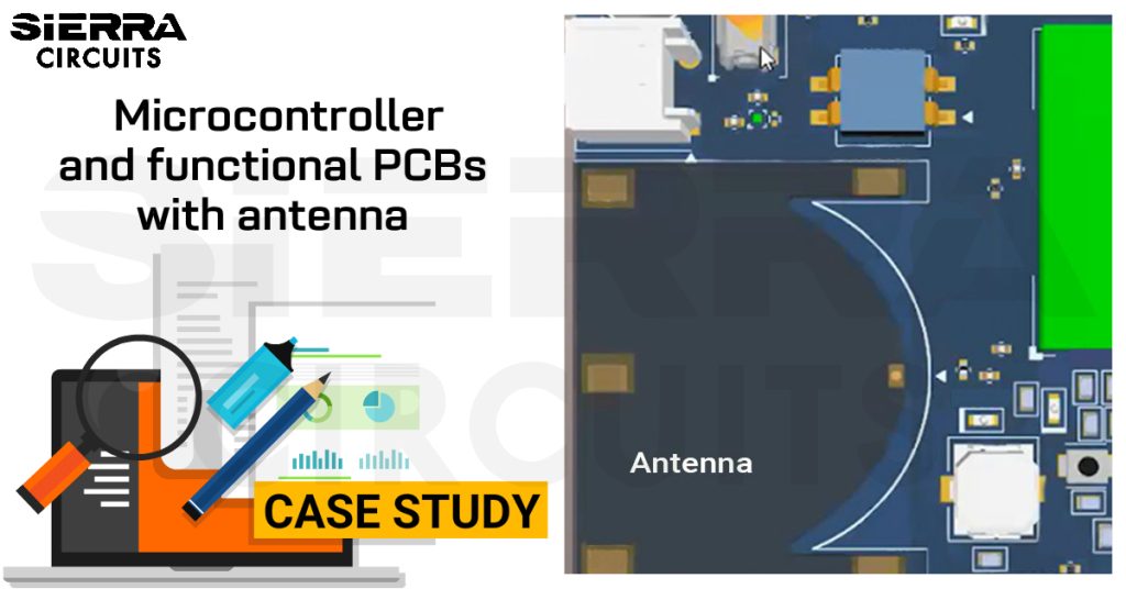
Case Study: Designing Microcontroller and Functional PCBs with an Antenna
We recently worked on a PCB design comprising 2 modules. Module 1 has a microcontroller, and module 2 hosts antenna […]
High Speed
Top 5 HDI PCB Routing Challenges and Ways to Mitigate Them
HDI designs pose complex routing challenges due to their tight spacing between components and traces. Using DRC settings in ... more »
HDI / Blind & Buried Vias
PCB Heat Dissipation Techniques by Keven Coates
Keven Coates shared his insights about PCB heat management at PCB West 2023. Keven Coates, a senior electrical ... more »
PCB Design
Case Study: Designing Microcontroller and Functional PCBs with an Antenna
We recently worked on a PCB design comprising 2 modules. Module 1 has a microcontroller, and module 2 ... more »
High Speed
Top 5 HDI PCB Routing Challenges and Ways to Mitigate Them
HDI designs pose complex routing challenges due to their tight spacing between components and traces. Using DRC settings in ... more »
HDI / Blind & Buried Vias
PCB Heat Dissipation Techniques by Keven Coates
Keven Coates shared his insights about PCB heat management at PCB West 2023. Keven Coates, a senior electrical ... more »
PCB Design
Decoupling Capacitor Placement Guidelines for PCB Design
Decoupling is a way of isolating signal components from composite signals based on frequency. Therefore, understanding which range ... more »
PCB Assembly
Controlled Impedance Routing Using Altium Designer
Controlled impedance is the characteristic impedance of a transmission line formed by PCB traces and its associated reference ... more »
Controlled Impedance
Component Placement Guidelines for PCB Design and Assembly
In the era of miniaturization and HDI PCBs, space optimization on the PCB might frequently affect proper component ... more »
PCB Assembly
11 Best High-Speed PCB Routing Practices
A PCB designer has a difficult task when it comes to routing a circuit board. Things get a ... more »
High Speed
Fabrication, Procurement, & Assembly. PCBs fully assembled in as fast as 5 days.
- Bundled together in an entirely-online process
- Reviewed and tested by Engineers
- DFA & DFM Checks on every order
- Shipped from Silicon Valley in as fast as 5 days
Fabrication. Procurement & Assembly optional. Flexible and transparent for advanced creators.
- Rigid PCBs, built to IPC-6012 Class 2 Specs
- 2 mil (0.002″) trace / space
- DFM Checks on every order
- 24-hour turn-times available
Complex technology, with a dedicated CAM Engineer. Stack-up assistance included.
- Complex PCB requirements
- Mil-Spec & Class 3 with HDI Features
- Blind & Buried Vias
- Flex & Rigid-Flex boards


