Speak to an Account Manager
![]() +1 (800) 763-7503
+1 (800) 763-7503
Related Categories — High Current » PCB Design
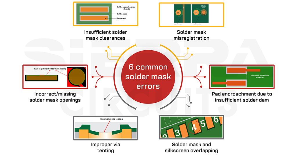
6 Common Solder Mask Errors Every PCB Designer Should Know
A solder mask is an insulation layer that covers conductive areas such as traces and pads. Inappropriate solder layer application […]
PCB Design
PCB Stack-up: Plan, Design, Manufacture and Repeat
Often ignored, it is important to understand the difference between an HDI stack-up and a standard stack-up. The ... more »
PCB Design
Case Study: Routing Microcontroller and BGA in Rigid-Flex PCBs
When routing microcontrollers and BGAs, you need to consider the trace spacing requirements of your design and clearance ... more »
Case Studies
6 Common Solder Mask Errors Every PCB Designer Should Know
A solder mask is an insulation layer that covers conductive areas such as traces and pads. Inappropriate solder ... more »
PCB Design
PCB Stack-up: Plan, Design, Manufacture and Repeat
Often ignored, it is important to understand the difference between an HDI stack-up and a standard stack-up. The ... more »
PCB Design
Case Study: Routing Microcontroller and BGA in Rigid-Flex PCBs
When routing microcontrollers and BGAs, you need to consider the trace spacing requirements of your design and clearance ... more »
Case Studies
Case Study: Designing a High-Current PCB with Voltage Doublers
PCBs with high operating current and voltage should adhere to specific layout rules to avert overheating and arcing ... more »
Case Studies
14 Aviation and Aerospace PCB Design Rules for High Reliability
When you’re designing aerospace and aviation PCBs, you need to consider structural strength, corrosion resistance, heat dissipation, and ... more »
Defense & Space
Best PCB Grounding Techniques for High-Power and HDI Designs
Incorporating proper PCB grounding techniques such as dedicated ground planes, ground vias, and galvanic isolation is critical in ... more »
PCB Design
Aerospace PCB Design Tips for Efficient Thermal Management
Advanced electronics in aerospace applications experience temperature fluctuations. A good aerospace PCB thermal management system isolates sections with ... more »
PCB Design
How Via Stitching Facilitates High-Current PCB Designs
Via stitching in high-current PCBs helps in creating proper ground connections, power distribution, and heat dissipation. These boards ... more »
PCB Design
Case Study: Designing 8 and 14-Layer HDI PCBs with Stacked Vias
Stacked vias are considered the most suitable solution for manufacturing HDI boards with advanced features. The configuration, with ... more »
Case Studies


Fabrication, Procurement, & Assembly. PCBs fully assembled in as fast as 5 days.
- Bundled together in an entirely-online process
- Reviewed and tested by Engineers
- DFA & DFM Checks on every order
- Shipped from Silicon Valley in as fast as 5 days

Fabrication. Procurement & Assembly optional. Flexible and transparent for advanced creators.
- Rigid PCBs, built to IPC-6012 Class 2 Specs
- 2 mil (0.002″) trace / space
- DFM Checks on every order
- 24-hour turn-times available

Complex technology, with a dedicated CAM Engineer. Stack-up assistance included.
- Complex PCB requirements
- Mil-Spec & Class 3 with HDI Features
- Blind & Buried Vias
- Flex & Rigid-Flex boards