Speak to an Account Manager
![]() +1 (800) 763-7503
+1 (800) 763-7503
Related Categories — PCB Design
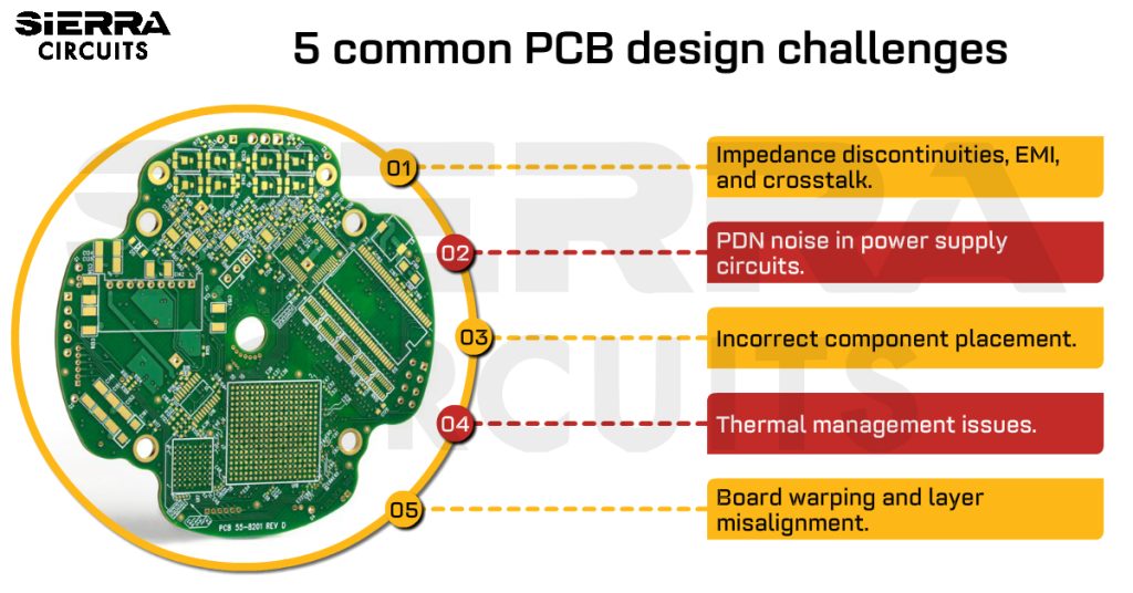
5 Typical PCB Design Challenges With Solutions for Engineers
With the rapid advancements in AI and IoT technologies, modern circuit designs demand careful attention to electrical, mechanical, and thermal […]
PCB Design
How to Design a Mixed-Signal PCB with Signal Integrity
Designing mixed-signal PCBs presents unique challenges in managing the interactions between digital and analog signals. Digital circuits generate ... more »
PCB Design
4 RF PCB Via Design Challenges with Layout Solutions
When designing vias for RF PCBs, their impedance should match the desired value in the operating bandwidth. To ... more »
High Speed
5 Typical PCB Design Challenges With Solutions for Engineers
With the rapid advancements in AI and IoT technologies, modern circuit designs demand careful attention to electrical, mechanical, ... more »
PCB Design
How to Design a Mixed-Signal PCB with Signal Integrity
Designing mixed-signal PCBs presents unique challenges in managing the interactions between digital and analog signals. Digital circuits generate ... more »
PCB Design
4 RF PCB Via Design Challenges with Layout Solutions
When designing vias for RF PCBs, their impedance should match the desired value in the operating bandwidth. To ... more »
High Speed
How to Autoroute a PCB Layout in KiCad using FreeRouting Plugin
The autorouting plugin in KiCad automates the PCB routing process by creating optimized signal paths. It allows you ... more »
PCB Design
10 Layout Tips for High-Speed and High-Current PCB Traces
When designing PCBs for frequencies over 5 GHz and current above 2A, trace design becomes paramount. To ensure ... more »
High Current
Microwave PCB Design Challenges and How to Overcome Them
Microwave PCB design presents unique challenges that differ from lower frequency boards. At microwave frequencies (1 GHz to ... more »
PCB Design
Microwave PCB Material Selection and CPW for Signal Integrity
Designing microwave boards involves meticulous selection of PCB materials, precise etching, and careful management of electromagnetic effects. These ... more »
PCB Design
How to Place Components in KiCad
In our previous tutorial, we demonstrated how to set up design rules in KiCad, which included how to ... more »
KiCad Tutorials
How to Draw and Design a PCB Schematic?
A schematic diagram is a logical and visual representation of an electrical circuit. It is the very first ... more »
PCB Design


Fabrication, Procurement, & Assembly. PCBs fully assembled in as fast as 5 days.
- Bundled together in an entirely-online process
- Reviewed and tested by Engineers
- DFA & DFM Checks on every order
- Shipped from Silicon Valley in as fast as 5 days

Fabrication. Procurement & Assembly optional. Flexible and transparent for advanced creators.
- Rigid PCBs, built to IPC-6012 Class 2 Specs
- 2 mil (0.002″) trace / space
- DFM Checks on every order
- 24-hour turn-times available

Complex technology, with a dedicated CAM Engineer. Stack-up assistance included.
- Complex PCB requirements
- Mil-Spec & Class 3 with HDI Features
- Blind & Buried Vias
- Flex & Rigid-Flex boards