Related Categories — HDI / Blind & Buried Vias » PCB Design
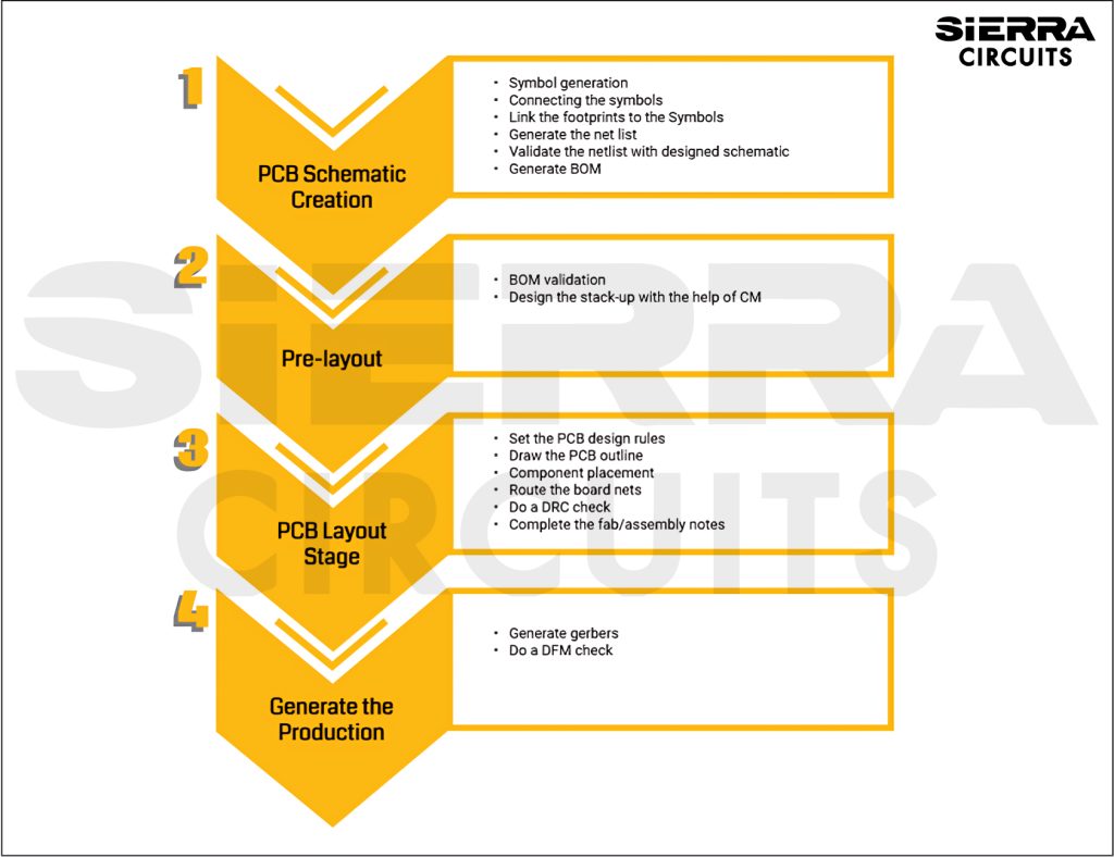
How to Design a PCB Layout
The design process of a PCB will essentially begin by creating a schematic. This schematic is then developed into a PCB layout using CAD software.
PCB Design
How to Handle Current Return Path for Better Signal Integrity
Before we start with today’s article, something needs to get engraved in your mind. If some current goes ... more »
PCB Design
Copper Wrap Plating Requirement for PCB Manufacturing
Multilayer PCB fabrication is a consistently evolving, progressively complex interplay of processes, design rules, and product specifications. In ... more »
PCB Design
How to Design a PCB Layout
The design process of a PCB will essentially begin by creating a schematic. This schematic is then developed ... more »
PCB Design
How to Handle Current Return Path for Better Signal Integrity
Before we start with today’s article, something needs to get engraved in your mind. If some current goes ... more »
PCB Design
Copper Wrap Plating Requirement for PCB Manufacturing
Multilayer PCB fabrication is a consistently evolving, progressively complex interplay of processes, design rules, and product specifications. In ... more »
PCB Design
9 Cost Drivers for Rigid Circuit Boards
Cost control steps should be taken in the early PCB production stages, including the actual circuit development stage. ... more »
PCB Assembly
What is the Difference Between Microstrip and Stripline in PCBs?
PCBs typically use two types of transmission lines: microstrips and striplines. Each of the transmission lines consists of ... more »
Controlled Impedance
Controlled Impedance Routing Using Altium Designer
Controlled impedance is the characteristic impedance of a transmission line formed by PCB traces and its associated reference ... more »
Controlled Impedance
Why Use Thermal Pads in PCB Design and Manufacturing
With the advancement of technology and miniaturization of devices, the heat generated per unit area on a PCB ... more »
PCB Design
Network Theory for Better PCB Design and Development
The study of resolving issues with electrical circuits and networks is called network theory. Network theory concepts are ... more »
PCB Design
What is a Prepreg in PCB Manufacturing?
As simple as it is, a prepreg is nothing but an insulation layer. Prepreg is a dielectric material ... more »
PCB Design
Fabrication, Procurement, & Assembly. PCBs fully assembled in as fast as 5 days.
- Bundled together in an entirely-online process
- Reviewed and tested by Engineers
- DFA & DFM Checks on every order
- Shipped from Silicon Valley in as fast as 5 days
Fabrication. Procurement & Assembly optional. Flexible and transparent for advanced creators.
- Rigid PCBs, built to IPC-6012 Class 2 Specs
- 2 mil (0.002″) trace / space
- DFM Checks on every order
- 24-hour turn-times available
Complex technology, with a dedicated CAM Engineer. Stack-up assistance included.
- Complex PCB requirements
- Mil-Spec & Class 3 with HDI Features
- Blind & Buried Vias
- Flex & Rigid-Flex boards


