Speak to an Account Manager
![]() +1 (800) 763-7503
+1 (800) 763-7503
Related Categories — High Current » PCB Design » PCB Layout » Power Integrity
Via Filling Techniques Designers Need to Know for PCB Fabrication
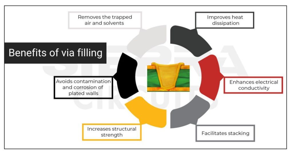
PCB via filling is a technique in which the plated hole is filled with a conductive or non-conductive material. It […]
PCB Manufacturing
13 Most Used PCB Layout Design Tools
PCB layout design tools assist you with schematic creation, layout design, trace routing, BOM validation, and design file ... more »
PCB Design
How to Design a PCB for 5G Wireless Applications
Designing PCBs for 5G and IoT applications demands high performance, low power consumption, and reliable connectivity. 5G surpasses ... more »
PCB Design
Via Filling Techniques Designers Need to Know for PCB Fabrication
PCB via filling is a technique in which the plated hole is filled with a conductive or non-conductive ... more »
PCB Manufacturing
13 Most Used PCB Layout Design Tools
PCB layout design tools assist you with schematic creation, layout design, trace routing, BOM validation, and design file ... more »
PCB Design
How to Design a PCB for 5G Wireless Applications
Designing PCBs for 5G and IoT applications demands high performance, low power consumption, and reliable connectivity. 5G surpasses ... more »
PCB Design
The Importance of PCB Line Spacing, Creepage, and Clearance
The PCB line spacing for creepage and clearance becomes an important factor from a product safety viewpoint when ... more »
High Current
Case Study: Designing Microcontroller and Functional PCBs with an Antenna
We recently worked on a PCB design comprising 2 modules. Module 1 has a microcontroller, and module 2 ... more »
High Speed
S-parameters Measurement Using a Vector Network Analyzer
Designing a board for operating frequencies higher than a few hundred MHz becomes challenging as it is difficult ... more »
PCB Design
Top 5 HDI PCB Routing Challenges and Ways to Mitigate Them
HDI designs pose complex routing challenges due to their tight spacing between components and traces. Using DRC settings in ... more »
HDI / Blind & Buried Vias
How to Determine the Impedance of a Circuit
Impedance impacts how signals propagate through the board, how power is exchanged between components, and how signals leak ... more »
Controlled Impedance
How to Reduce Ringing in Your PCB Designs
PCB ringing is an unwanted oscillation of voltage or current in a circuit board. During the signal transition ... more »
PCB Design


Fabrication, Procurement, & Assembly. PCBs fully assembled in as fast as 5 days.
- Bundled together in an entirely-online process
- Reviewed and tested by Engineers
- DFA & DFM Checks on every order
- Shipped from Silicon Valley in as fast as 5 days

Fabrication. Procurement & Assembly optional. Flexible and transparent for advanced creators.
- Rigid PCBs, built to IPC-6012 Class 2 Specs
- 2 mil (0.002″) trace / space
- DFM Checks on every order
- 24-hour turn-times available

Complex technology, with a dedicated CAM Engineer. Stack-up assistance included.
- Complex PCB requirements
- Mil-Spec & Class 3 with HDI Features
- Blind & Buried Vias
- Flex & Rigid-Flex boards