Speak to an Account Manager
![]() +1 (800) 763-7503
+1 (800) 763-7503
Related Categories — High Current » PCB Design » PCB Layout » Power Integrity
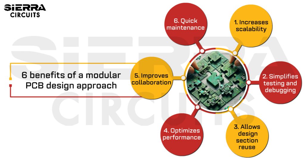
How Modular PCB Design Method Simplifies Complex Layouts
In a modular PCB design method, a complex circuit board is divided into smaller modules. Each performs a specific function […]
PCB Design
How to Pick RF PCB Materials: 6 Important Factors to Consider
When designing RF PCBs, selecting the right material is pivotal for achieving optimal board performance. The properties of ... more »
High Speed
Antenna Integration and RF Design Guidelines for 5G PCBs
Designing an RF PCB for 5G devices requires a deep understanding of antenna integration, high-frequency signal handling, precise ... more »
PCB Design
How Modular PCB Design Method Simplifies Complex Layouts
In a modular PCB design method, a complex circuit board is divided into smaller modules. Each performs a ... more »
PCB Design
How to Pick RF PCB Materials: 6 Important Factors to Consider
When designing RF PCBs, selecting the right material is pivotal for achieving optimal board performance. The properties of ... more »
High Speed
Antenna Integration and RF Design Guidelines for 5G PCBs
Designing an RF PCB for 5G devices requires a deep understanding of antenna integration, high-frequency signal handling, precise ... more »
PCB Design
How to Reduce Your PCB Assembly Cost
Maintaining the highest quality standards in boards while simultaneously reducing PCB assembly costs can be an ongoing struggle ... more »
PCB Assembly
Case Study: Designing Loose-Leaf Rigid-Flex PCB Stack-up for Enhanced Flexibility
When designing a flex circuit board, balancing structural reliability and signal integrity is paramount. In our recent project, ... more »
Flex PCBs
Flex PCB Design Guidelines Part 2: Optimizing Layout for Manufacturing
In this webinar, we discuss flex PCB design guidelines for manufacturing. The flex PCBs offer many advantages for ... more »
Flex PCBs
5 PCB Trace Termination Techniques to Reduce Signal Reflections
PCB trace termination is crucial for maintaining signal integrity in your designs. Unterminated traces can lead to issues ... more »
PCB Design
Case Study: Resolving EMI and PCB Routing Issues in a Medical Optical Scanner
Our PCB design engineers worked on a medical circuit board for a healthcare device: an advanced optical scanner ... more »
Case Studies
4 Common PDN Design Challenges and How to Resolve Them
An efficient PDN design in PCBs ensures a stable power supply and consistent voltage levels across all components. ... more »
PCB Design


Fabrication, Procurement, & Assembly. PCBs fully assembled in as fast as 5 days.
- Bundled together in an entirely-online process
- Reviewed and tested by Engineers
- DFA & DFM Checks on every order
- Shipped from Silicon Valley in as fast as 5 days

Fabrication. Procurement & Assembly optional. Flexible and transparent for advanced creators.
- Rigid PCBs, built to IPC-6012 Class 2 Specs
- 2 mil (0.002″) trace / space
- DFM Checks on every order
- 24-hour turn-times available

Complex technology, with a dedicated CAM Engineer. Stack-up assistance included.
- Complex PCB requirements
- Mil-Spec & Class 3 with HDI Features
- Blind & Buried Vias
- Flex & Rigid-Flex boards