Speak to an Account Manager
![]() +1 (800) 763-7503
+1 (800) 763-7503
Related Categories — High Current » PCB Design » PCB Layout » Power Integrity
How to Reduce Parasitic Capacitance in PCB Layout
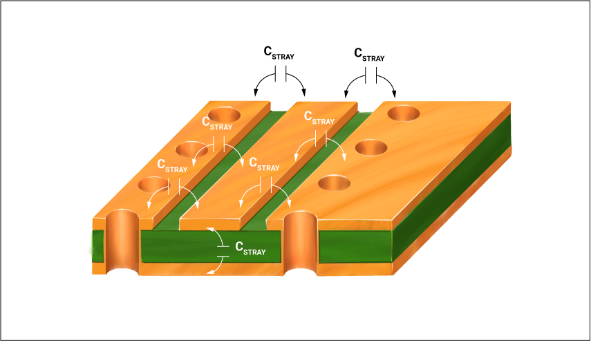
A PCB consists of several parallelly spanned conductors, say traces, separated by an insulator. These traces, along with dielectric material, form a capacitor, resulting in an unwanted parasitic capacitance or stray capacitance effect.
PCB Design
What Is PCIe (PCI Express)?
Innovation in computing is an ongoing trend that keeps growing exponentially in today's digital world. With data transfer ... more »
PCB Design
Case Study: Enabling the LiDAR Industry
LiDAR is an emerging technology along the lines of radar and sonar which identifies and maps objects besides ... more »
Case Studies
How to Reduce Parasitic Capacitance in PCB Layout
A PCB consists of several parallelly spanned conductors, say traces, separated by an insulator. These traces, along with ... more »
PCB Design
What Is PCIe (PCI Express)?
Innovation in computing is an ongoing trend that keeps growing exponentially in today's digital world. With data transfer ... more »
PCB Design
Case Study: Enabling the LiDAR Industry
LiDAR is an emerging technology along the lines of radar and sonar which identifies and maps objects besides ... more »
Case Studies
Choosing IPC Class for Medical Flex PCBs
Flex PCBs are widely used in medical devices and wearables as they offer some great advantages. The demand ... more »
PCB Design
How to Export Gerber and Design Files in Allegro
After the layout, the design is converted into a standard file format called Gerber files. Most PCB makers ... more »
PCB Design
High Voltage Circuit Boards and Safety Standards
High voltage board designing requires an understanding of international safety standards such as IPC 2221A and UL 60950-1. ... more »
PCB Design
How to Design a PCB Layout
The design process of a PCB will essentially begin by creating a schematic. This schematic is then developed ... more »
PCB Design
How to Handle Current Return Path for Better Signal Integrity
Before we start with today’s article, something needs to get engraved in your mind. If some current goes ... more »
PCB Design
Copper Wrap Plating Requirement for PCB Manufacturing
Multilayer PCB fabrication is a consistently evolving, progressively complex interplay of processes, design rules, and product specifications. In ... more »
PCB Design


Fabrication, Procurement, & Assembly. PCBs fully assembled in as fast as 5 days.
- Bundled together in an entirely-online process
- Reviewed and tested by Engineers
- DFA & DFM Checks on every order
- Shipped from Silicon Valley in as fast as 5 days

Fabrication. Procurement & Assembly optional. Flexible and transparent for advanced creators.
- Rigid PCBs, built to IPC-6012 Class 2 Specs
- 2 mil (0.002″) trace / space
- DFM Checks on every order
- 24-hour turn-times available

Complex technology, with a dedicated CAM Engineer. Stack-up assistance included.
- Complex PCB requirements
- Mil-Spec & Class 3 with HDI Features
- Blind & Buried Vias
- Flex & Rigid-Flex boards