Related Categories — High Current » PCB Design
Next-Gen Memory DDR5 and Signal Integrity in High-Speed PCBs with Stephen Slater
Stephen Slater during DesignCon-2022 gave us a wonderful chance to talk about his views on next-gen memory and signal integrity […]
High Speed
VNA or TDR: The Right Time-Domain Measurement by Mike Resso
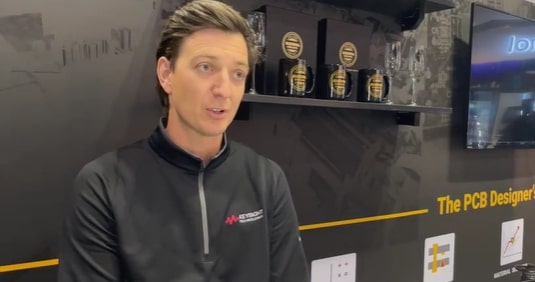
We got an opportunity to talk to Mike Resso of Keysight during DesignCon 2022 . Watch the video ... more »
PCB Design
PCB Layout, Model Extractions, and Simulations by Matthew Harms
During DesignCon 2022, we interviewed Matthew Harms of EMA Design Automation to understand more about model extractions and ... more »
PCB Design
Next-Gen Memory DDR5 and Signal Integrity in High-Speed PCBs with Stephen Slater
Stephen Slater during DesignCon-2022 gave us a wonderful chance to talk about his views on next-gen memory and ... more »
High Speed
VNA or TDR: The Right Time-Domain Measurement by Mike Resso
We got an opportunity to talk to Mike Resso of Keysight during DesignCon 2022 . Watch the video ... more »
PCB Design
PCB Layout, Model Extractions, and Simulations by Matthew Harms
During DesignCon 2022, we interviewed Matthew Harms of EMA Design Automation to understand more about model extractions and ... more »
PCB Design
DDR4, Signal Integrity, and Power Integrity in PCB Design with Benjamin Dannan
We got an opportunity to pick Benjamin Dannan’s brain during DesignCon 2022. Watch the video to find out ... more »
PCB Design
Schematic and Netlist Checks to Ensure Error-Free Designs
Schematic and netlist checks are performed to check schematic symbols, verify electrical characteristics, and analyze the netlist consistency. ... more »
PCB Design
How to Design a Via with Current Carrying Capacity
The word ‘via’ is originally a Latin word that means road or way. In designing PCBs, vias play ... more »
PCB Design
HDI Standard Board Tools for a Better PCB design
Unlike traditional PCBs, HDI boards can obtain interconnections through blind vias, buried vias, and microvias, instead of just ... more »
HDI / Blind & Buried Vias
ODB++: An Intelligent Format for PCB Designs
A side-by-side comparison of ODB++, Gerbers, and IPC-2581 PCB design formats. While ODB++ and IPC-2581 have recently been ... more »
PCB Design
Common Problems Associated With Gerber Files
The most common problems seen in Gerber files include design mismatch, insufficient clearances, obsolete file formats, unregistered layers, ... more »
PCB Design
Fabrication, Procurement, & Assembly. PCBs fully assembled in as fast as 5 days.
- Bundled together in an entirely-online process
- Reviewed and tested by Engineers
- DFA & DFM Checks on every order
- Shipped from Silicon Valley in as fast as 5 days
Fabrication. Procurement & Assembly optional. Flexible and transparent for advanced creators.
- Rigid PCBs, built to IPC-6012 Class 2 Specs
- 2 mil (0.002″) trace / space
- DFM Checks on every order
- 24-hour turn-times available
Complex technology, with a dedicated CAM Engineer. Stack-up assistance included.
- Complex PCB requirements
- Mil-Spec & Class 3 with HDI Features
- Blind & Buried Vias
- Flex & Rigid-Flex boards


