Related Categories — High Speed » KiCad Tutorials
Techniques to Measure and Avoid Jitter in PCBs
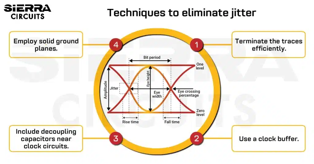
A signal’s deflection from its ideal rising and falling edges is called jitter in PCBs. Jitter in clock signals can […]
High Speed
4 RF PCB Via Design Challenges with Layout Solutions
When designing vias for RF PCBs, their impedance should match the desired value in the operating bandwidth. To ... more »
High Speed
10 Layout Tips for High-Speed and High-Current PCB Traces
When designing PCBs for frequencies over 5 GHz and current above 2A, trace design becomes paramount. To ensure ... more »
High Current
Techniques to Measure and Avoid Jitter in PCBs
A signal’s deflection from its ideal rising and falling edges is called jitter in PCBs. Jitter in clock ... more »
High Speed
4 RF PCB Via Design Challenges with Layout Solutions
When designing vias for RF PCBs, their impedance should match the desired value in the operating bandwidth. To ... more »
High Speed
10 Layout Tips for High-Speed and High-Current PCB Traces
When designing PCBs for frequencies over 5 GHz and current above 2A, trace design becomes paramount. To ensure ... more »
High Current
How to Create a Schematic for High-Speed Designs in KiCad
KiCAD is a widely used free Electronic Design Automation (EDA) software. The software is mainly used as a ... more »
High Speed
9 Factors that Impact RF PCB Designs and Tips to Resolve Them
An RF PCB design is a bit different from a conventional board. It is more susceptible to signal ... more »
High Speed
How to Pick RF PCB Materials: 6 Important Factors to Consider
When designing RF PCBs, selecting the right material is pivotal for achieving optimal board performance. The properties of ... more »
High Speed
Case Study: Designing Microcontroller and Functional PCBs with an Antenna
We recently worked on a PCB design comprising 2 modules. Module 1 has a microcontroller, and module 2 ... more »
High Speed
How to Handle Crosstalk in High-Speed PCB Designs
Signal integrity measurements have become a critical step in the process of developing digital systems. Signal integrity problems ... more »
High Speed
High-Speed and HDI PCB Design Strategies by Syed Ubaid Ali Warsi
Syed Ubaid Ali Warsi, the owner of Wavetroniks, provided his insights into high-speed and HDI PCB design strategies ... more »
HDI / Blind & Buried Vias
Fabrication, Procurement, & Assembly. PCBs fully assembled in as fast as 5 days.
- Bundled together in an entirely-online process
- Reviewed and tested by Engineers
- DFA & DFM Checks on every order
- Shipped from Silicon Valley in as fast as 5 days
Fabrication. Procurement & Assembly optional. Flexible and transparent for advanced creators.
- Rigid PCBs, built to IPC-6012 Class 2 Specs
- 2 mil (0.002″) trace / space
- DFM Checks on every order
- 24-hour turn-times available
Complex technology, with a dedicated CAM Engineer. Stack-up assistance included.
- Complex PCB requirements
- Mil-Spec & Class 3 with HDI Features
- Blind & Buried Vias
- Flex & Rigid-Flex boards


